When installing drivers for a recently installed PCI card:
Month: November 2013
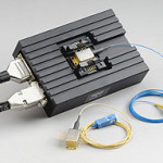
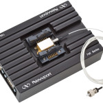
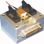
Butterfly laser diode mount
We've put together a few of these butterfly laser-diode mount + driver combos. It combines a heat-sinked butterfly mounted laser-diode with a current/temperature controller by Wavelength Electronics. The assembly is low enough to fit into a 1U (~44 mm) high 19" rack-enclosure.
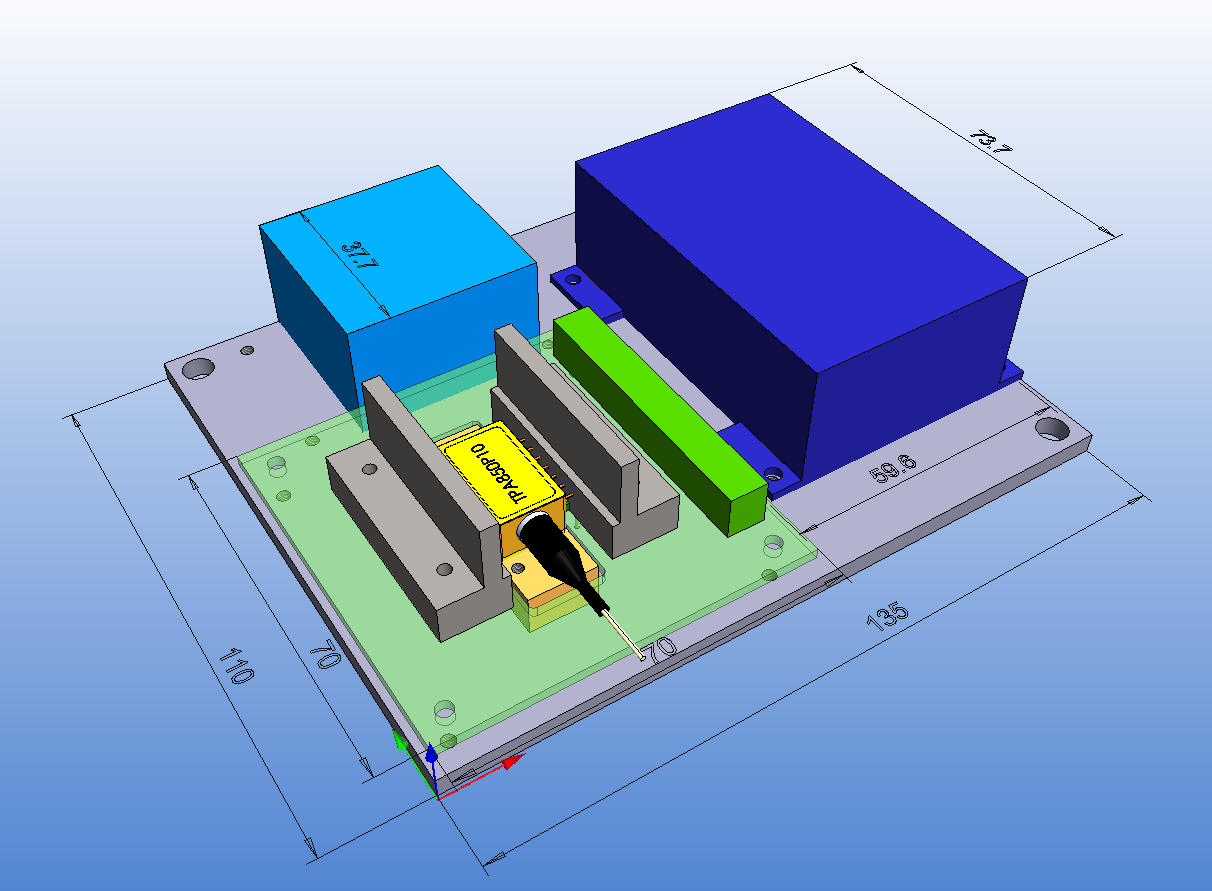
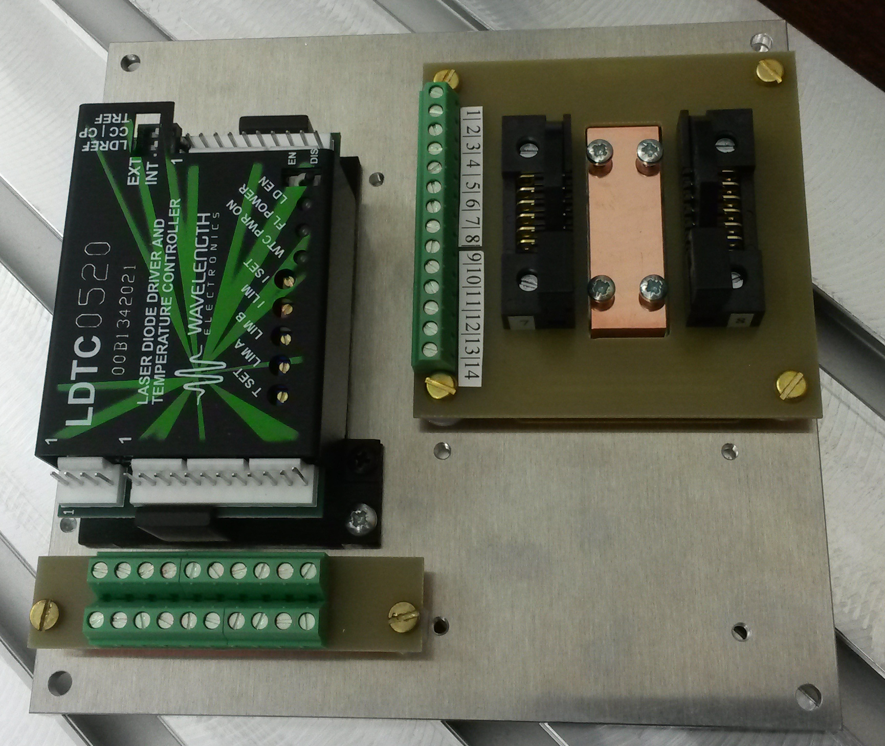
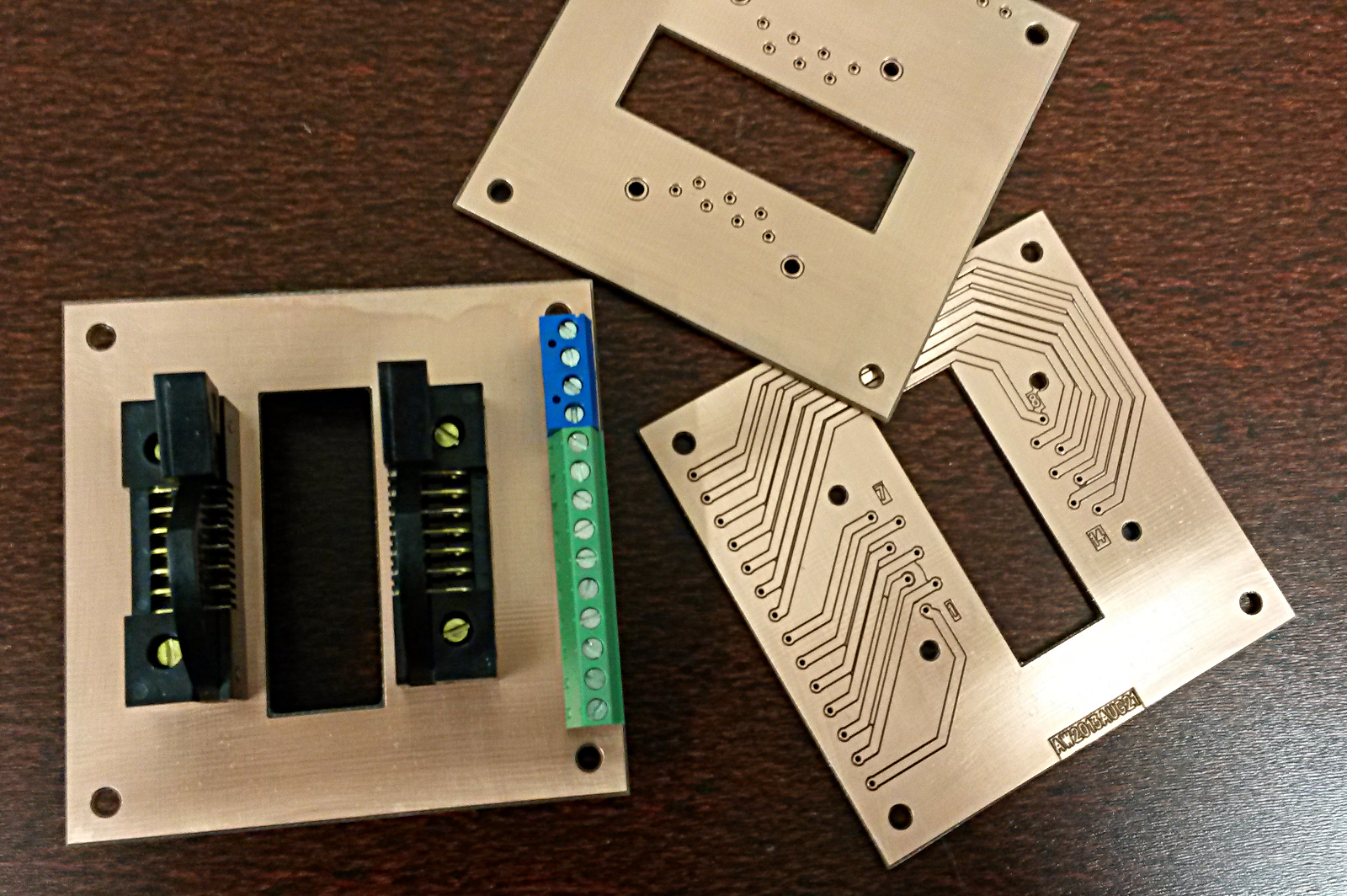
The 14-pin laser-package (yellow) is held in place by ZIF clamps/sockets 5253-100-07S (standard) and 5253-100-07R (reverse) from from Azimuth Electronics (grey in the CAD drawing, black in real life). The Wavelength Electronics LDTC driver controls both the laser current and temperature using the laser's own on-board TEC and thermistor. The base-plate has additional room for a heatsink and a fan, but so far I think nobody has used this feature. Semiconductor lasers have about 30% efficiency, so with anything under 1 W of optical output the dissipated heat should stay below 3-5 W.
The metal parts are an aluminium base-plate (see bfly_mount_v1_plate_2013aug26 and the newer bfly_mount_v2_plate_2013nov1). A copper riser-block (bfly_mount_v1_riser-block_2013aug26) sits on top of the base-plate and provides good heat-conduction from the laser package to the base-plate. The riser-block and the laser are bolted together with M2.5 bolts/screws (allen-bolts would be more stylish - I know!). I also made a mechanical drawing for the PCB bfly_mount_v1_pcb_drawing.
The PCB has no electronics on it (see bfly_mount_v1_schematic_2013sep3), the pins from the Azimuth sockets are just routed to 150 mil pitch screw terminals.
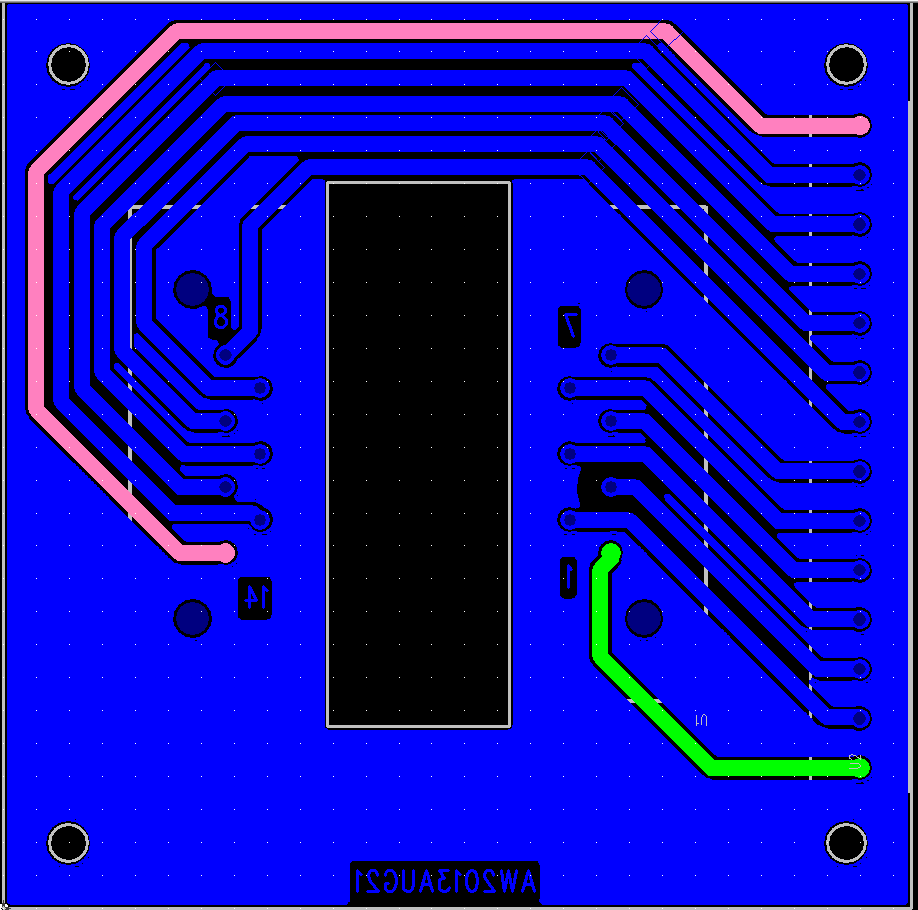
See also gerbers for manufacturing: butterfly_pcb_v1_camfiles or the slightly modified version dated 2013-11-14 butterfly_v3_camfiles
There's an additional mini-pcb for screw-terminals on the input side of the LDTC controller. screwterminal_camfiles_2013-09-12
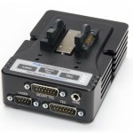
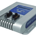
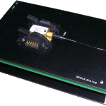
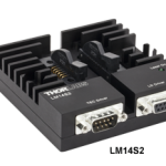
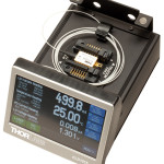
Our in-house design won't win any prizes for design or style, but it does the job. Here are a few pictures of commercial butterfly mounts. Some combine the current/temperature driver with the mount, others just have D-sub connectors for external current/temperature controllers.
NTP failure detection
Update: Here's how the graph looks like when NTP traffic is enabled again:
A computer that doesn't receive NTP traffic for a while will have its system time drift quite a lot.
In the absence of NTP (UDP port 123) traffic, we can try to roughly ask for the current time over HTTP using wget from google with this shell script:
#!/bin/sh
/usr/bin/wget --no-cache -S -O /dev/null google.com 2>&1 | \
/bin/sed -n -e '/ *Date: */ {' -e s///p -e q -e '}' |
This outputs a string such as "Sat, 23 Nov 2013 09:14:45 GMT"
Now we can put together a python script that calls this shell script, converts the text-format time-stamp into UTC seconds, and compares against the system time. For plotting we then store the time-error in an RRDTool database. This script is called once per minute using cron.
import subprocess import time import datetime import rrdtool import syslog args = ['googletime.sh'] datetimestring = subprocess.check_output(args) syslog.syslog( "googletime {0}".format(datetimestring)) # input: Sat, 23 Nov 2013 09:18:02 GMT # output: 1385191082.0 (seconds since 1.1.1970) timestamp = time.mktime( time.strptime(datetimestring, '%a, %d %b %Y %H:%M:%S GMT\n')) # system time, e.g.: 1385191082.0 stime = time.mktime( time.gmtime() ) # should be zero, if all is well terror = stime-timestamp # store the measured error in a database datastring = 'N:{0}'.format(str(terror)) # 'N:1234' syslog.syslog( "rrd update: {0}".format(datastring) ) ret = rrdtool.updatev( "time_error.rrd" ,datastring) syslog.syslog( "rrd updatev: {0}".format(ret) ) |
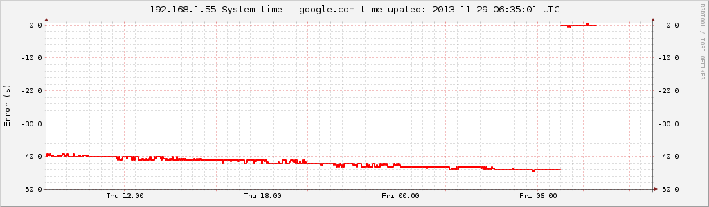
Once we have all the values in our time_error.rrd database we can plot them with rrdtool graph. This is what I get:
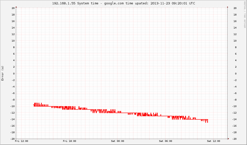
There is about -4 seconds of drift during 24 hours, or 46 us/s (46 ppm). If the drift is steady we can guess that the computer was on time 14/4 = ~4 days ago.
The script for creating the rrdtool database is this:
import rrdtool import time # DS:ds-name:GAUGE | COUNTER | DERIVE | ABSOLUTE:heartbeat:min:max data_sources=[ 'DS:TERROR:GAUGE:70:U:U'] # RRA:AVERAGE | MIN | MAX | LAST:xff:steps:rows utcsecs = int( time.time() ) pts_day= 24*60 primary = 'RRA:AVERAGE:0.5:1:{0}'.format(pts_day) # 2016 points rrdtool.create( 'time_error.rrd', # filename '--start', str(utcsecs), # when to start '--step', '60', # step between datapoints data_sources, primary) |
And the graph is created by this script. I am using the simple python-rrdtool python bindings - the object-oriented python-pyrrd may have neater syntax and be more pythonic.
import rrdtool import time graphname = '/var/www/test.png' day = 24*3600 span = 1*day starttime = int(time.time()-span) endtime = int( time.time() + 0.1*span) updatestamp = time.strftime("%Y-%m-%d %H:%M:%S UTC", time.gmtime(time.time())) graphtitle = '192.168.1.55 System time - google.com time upated: '+updatestamp rrdtool.graph( graphname, '--start', str(starttime), '--end',str(endtime), '--title',graphtitle, '--width',str(1024), '--height',str(600), '--full-size-mode', '--upper-limit',str(20), '--lower-limit',str(-20), '--vertical-label','Error (s)', '--right-axis', '1:0', 'DEF:terror=time_error.rrd:TERROR:AVERAGE', 'LINE2:terror#FF0000') |
Praha


GPIB on Linux
Update 2015 June: additions for Ubuntu 14.04LTS (where a symbolic link is required), and for the NI-USB-B dongle (which needs firmware loading). See also: Using the National Instruments GPIB-USB-B on linux
Notes on how to use GPIB from python on Ubuntu 12.04LTS. Tested with National Instruments USB-GPIB device and a recently bought NI GPIB PCI-E card.
- Get linux-gpib source from http://sourceforge.net/projects/linux-gpib/
- Building the python bindings requires libboost-python (and maybe libboost-python-dev)
- build linux-gpib by running: ./configure, make, sudo make install
- edit /etc/gpib.conf to fit your hardware. The default config board_type = "ni_pci" seems to work with the NI PCI-E card. For the USB-GPIB device we need board_type = "ni_usb_b"
- load the kernel module, for the PCI-E card this is sudo modprobe tnt4882, for the USB-dongle this is sudo modprobe ni_usb_gpib
- On Ubuntu 14.04LTS the library that gpib_config is linked against is installed in a location where the binary doesn't find it. The fix is to add a symbolic link in /lib/
/lib$ sudo ln -s /usr/local/lib/libgpib.so.0 libgpib.so.0 - configure: sudo gpib_config --minor 0 this reads and parses /etc/gpib.conf so it needs to be re-done if something is changed in gpib.conf
- If gpib_config fails, and you have the older/slower NI-USB-B dongle, then you need to first load the firmware. This seems to not be required with the newer NI-USB-HS (to be confirmed?). Firmware loading requires fxload and the firmware from http://linux-gpib.sourceforge.net/firmware/. Find out where your USB-dongle is with lsusb and then load the firmware with something like:
fxload -D /proc/bus/usb/001/002 -I niusbb_firmware.hex -s niusbb_loader.hex where you replace /001/002 with the numbers for your USB device. Now gpib_config should work. - By default only members of the gpib-group can use gpib, and only root has access to /etc/gpib0. If we want normal users to use gpib, add them to the gpib group (on Ubuntu the graphical user&group editor is gnome-system-tools)
- Test!
note: If "import gpib" fails in python you might have forgotten to install libboost-python before building linux-gpib. Python bindings will not be built&installed unless you have libboost-python.
I have two devices, so I've configured them like this in gpib.conf
/* agilent mux/dmm */ device { minor = 0 /* first gpib-card/usb-dongle */ name = "dmm" pad = 8 /* primary address, configure on instrument front-panel*/ sad = 0 /* secondary address, always zero? */ } /* kikusui psu controller */ device { minor = 0 name = "kikusui" pad = 1 sad = 0 } |
And now we can try some python:
1 2 3 4 5 6 7 8 9 10 11 12 13 14 15 16 17 18 19 20 | import gpib import time dmm= gpib.find("dmm") # define in /etc/gpib.conf kik= gpib.find("kikusui") def query(handle, command, numbytes=100): gpib.write(handle,command) time.sleep(0.1) response = gpib.read(handle,numbytes) return response print query(dmm,"*IDN?") print query(kik,"*IDN?") gpib.close(dmm) gpib.close(kik) # output: # HEWLETT-PACKARD,34970A,0,13-2-2 # KIKUSUI ELECTRONICS CORP.,PIA4830,0,2.20 |
DC-Bias Amplifier
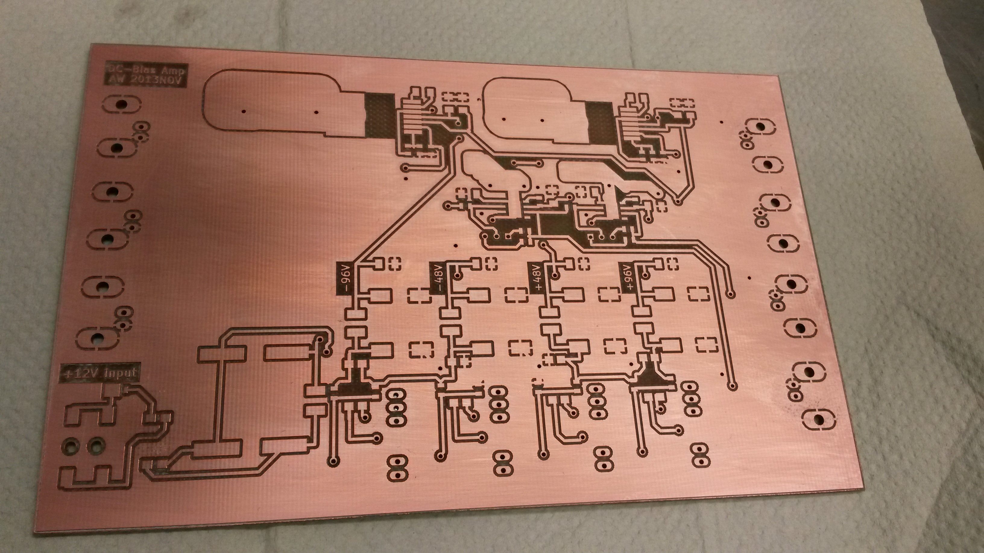
I've put together the first version of a DC-bias amplifier used for applying four DC-voltages to the trim electrodes of an ion trap. The axial voltages required are low, and they are applied symmetrically as +Vz and -Vz. The transverse voltages (X and Y) however can be as high as 100 V. Two high-voltage op-amps PA340CC are used for the X and Y channels, while the -Z and +Z output voltages are produced by two OPA454 op-amps. The amplifier has three +/-10 V inputs (Vx, Vy, Vz), and produces four outputs designed to be 10*Vx, 10*Vy, -Vz, and +Vz.
The amplifier circuit itself is very simple with the two PA340CC's in non-inverting configuration with a gain of 10, and the two OPA454's in inverting configuration, connected in series, with a gain of 1. The bandwidth requirement is very low, and the load should be equivalent to an open circuit - hence high 100k output resistor and a cap producing a 16 Hz low-pass filter on the output
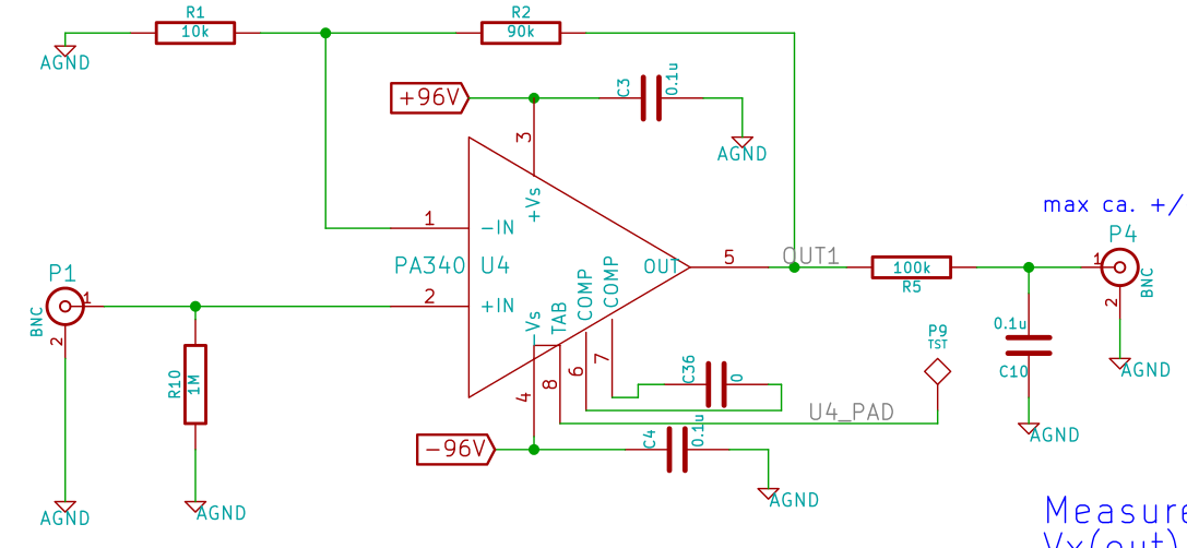
See full schematic as PDF: bias_amp_v0
The high-voltage DC-rails for the op-amps are produced by connecting four +/-24 V DC-to-DC converters in series. This allows powering the amplifier from a single +12VDC powersupply-brick, and in theory produces +/-48 V for the lower-voltage op-amps and +/-96 V for the high-voltage op-amps.
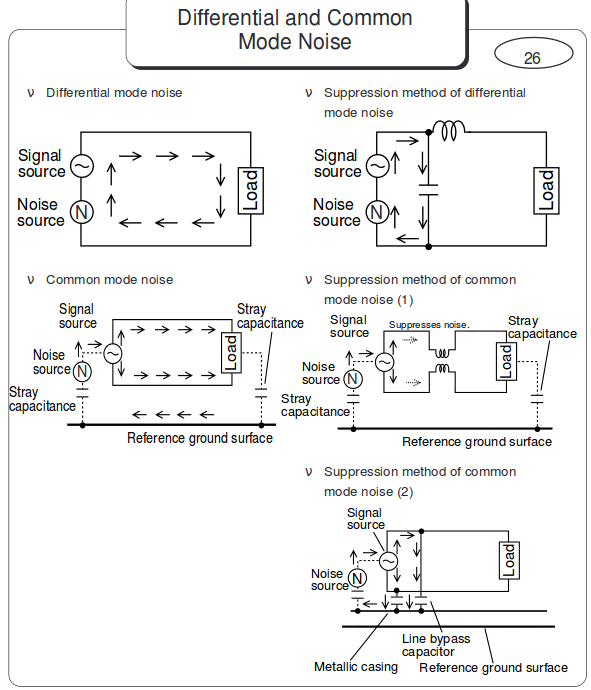
One issue with DC-to-DC converters is that they produce both differential and common-mode noise on the output. Conventional filter-caps or Pi-filtering removes the differential noise but does nothing to the common-mode noise. A common mode choke and/or filtering capacitors across the isolation-barrier to the input-side ground are required to remove the common-mode noise. Here's a picture from a Murata app-note that explains the idea:
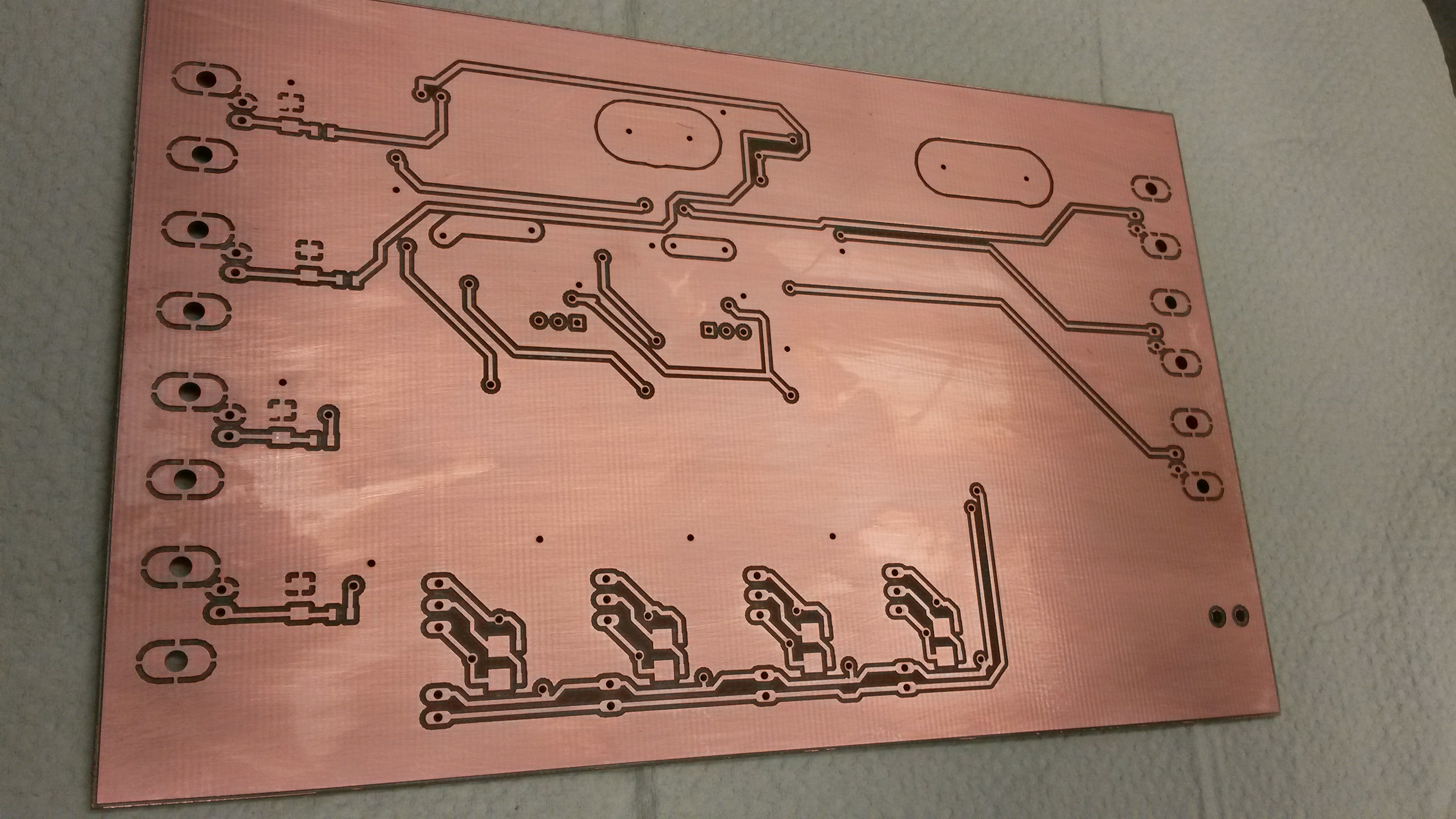
The components fit comfortably on a 100mm by 160mm PCB like this:
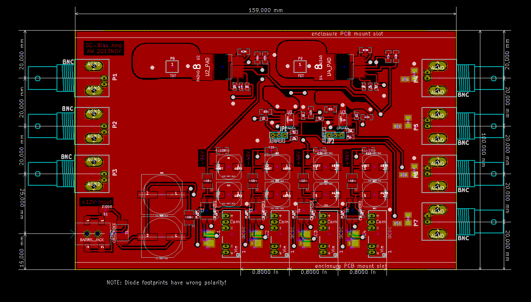
Only top Cu-layer shown. Why doesn't Kicad have built-in PDF export for the PCB-editor (like in the schematic-editor)?
Gerber and Excellon files from Kicad worked without problems with CircuitCAM for producing toolpaths for BoardMaster that runs our LPKF PCB mill. The PCB after milling, rubbed with steel-wool, cleaned with isopropanol, and then coated with PRF202.
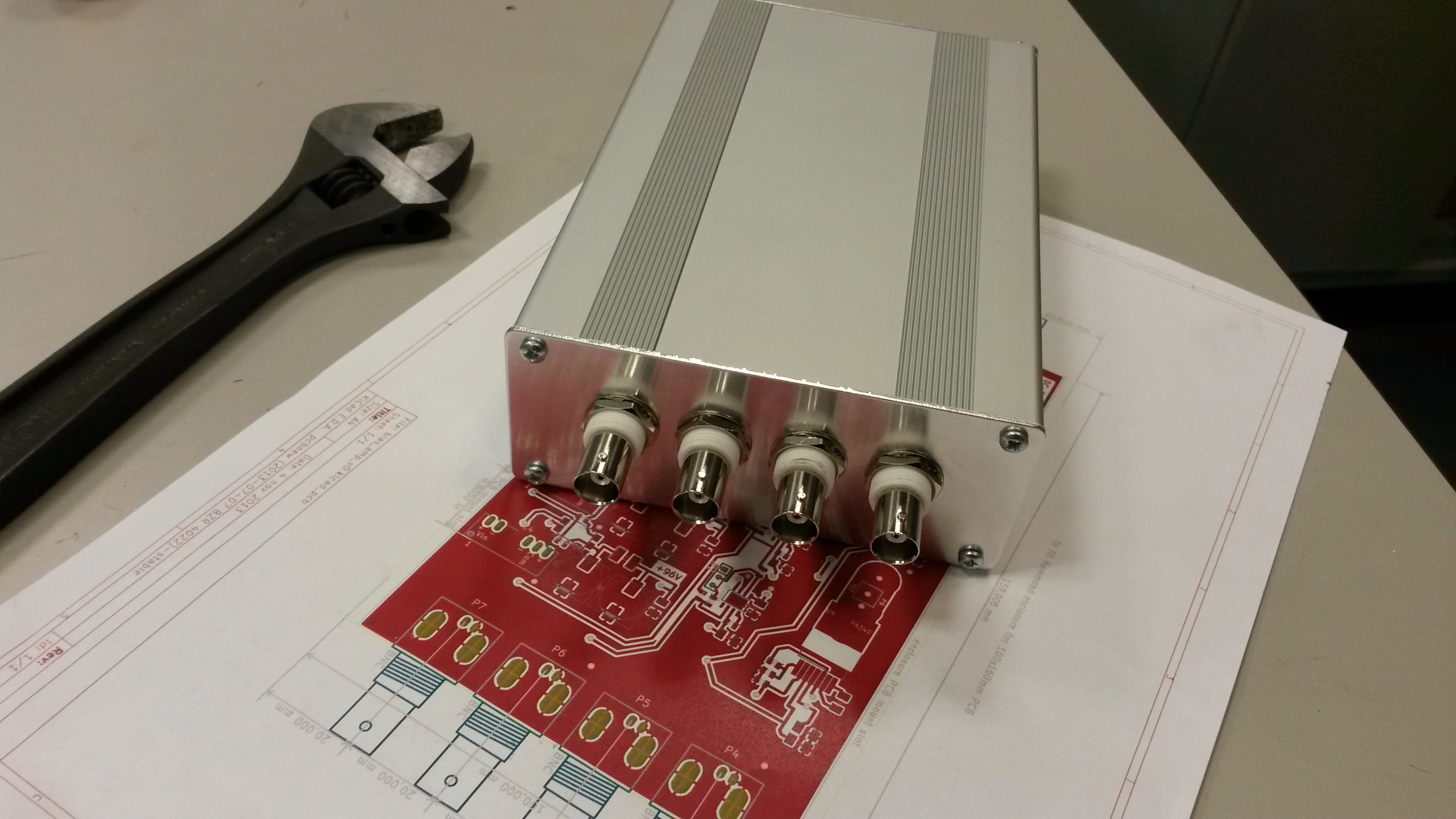
Components soldered, and board fit into an enclosure (Multicomp MCRECS160):
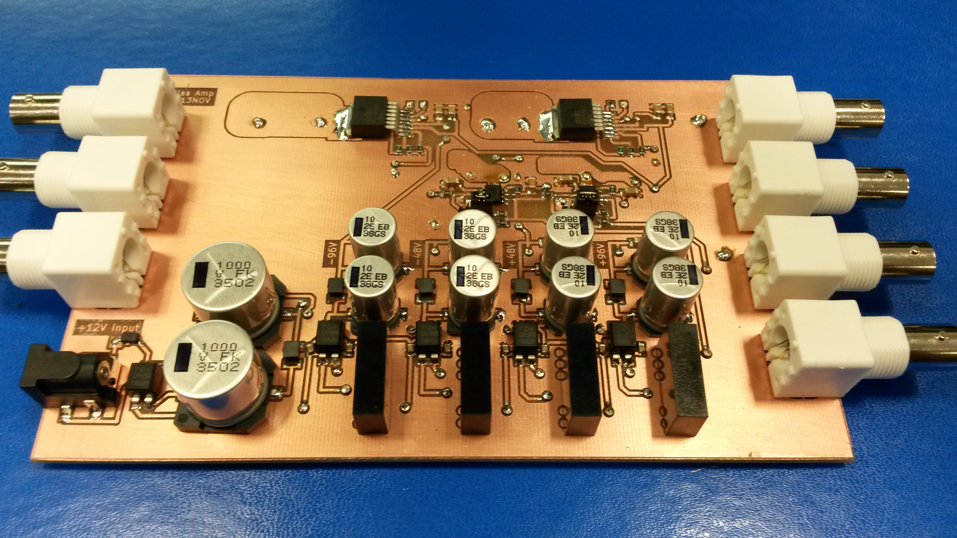
When powered up the DC-rails measured slightly lower voltages than expected. I got -89V, -44V, +44V, and +89V. The no-load input current was surprisingly high at 190mA. The dc-to-dc converters have a no-load spec of 20mA, so this explains about half of the measured current. The op-amps have a quiescent current of 3.2 mA @ +/48V for OPA454 and 2.2 mA @ +/-96V for PA340. So the 'middle' DC-to-DC converters that power all four op-amps should have 2*(3.2+2.2)= 10.8mA load at 48V and the 'side' converters only 2*3.2=6.4mA at 48V. That's 17.2 mA at 48V together, which should correspond to 84 mA at 12V if we trust the 82% efficiency number from the datasheet. So we can explain 80mA as no-load current and 84 mA from the quiescent current of the op-amps. That's 164 mA together, which is about 85% of the 190mA number shown by the powersupply. If my reasoning here is way off please comment below!
Initial measurements shows that the outputs behave roughly as designed. The high-voltage outputs max out at about +/- 85 V. Note that the 10 MOhm input of a DMM measures only 99% of the actual output voltage, due to the high 100k output impedance of the amplifier.
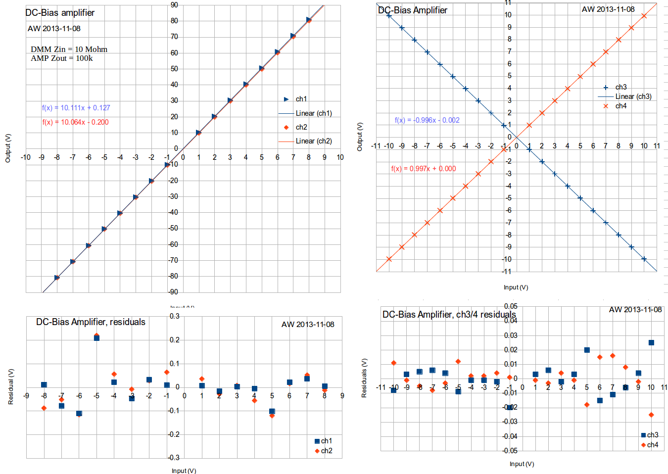
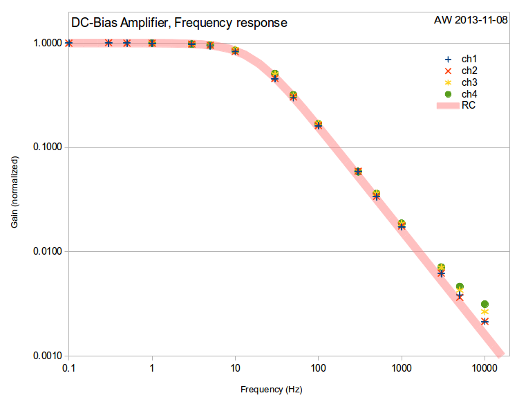
The frequency response is completely dominated by the 16 Hz low-pass RC-filter on the output, although the op-amps have unity-gain bandwidths of ~10 and ~2 MHz.
Notes and comments:
- This was the first board I designed with Kicad. It works rather well, and new enhancements are already on the way. The export of a netlist from the schematic-editor to the PCB-editor could be a bit smoother, and the footprint assignment should probably be done in the schematic-editor and the current CvPCB footprint-assignment bypassed.
- I used quite conservative design rules(mils): clearance 16, track 25, via 55, via drl 35. This seems to work quite well. The clearance could be reduced down towards 8 mils which is the minimum isolation clearance the PCB-mill can produce. Kicad automatically enforces clearance and via design rules interactively while routing the tracks - this is probably good once you get used to it.
- I messed up the polarity of the diode footprints - should be fixed if a second version is built.
- Linear regulators could be added on the DC-rails, after the pi-filters. Or perhaps a shunt regulator on the high-voltage rails.
- With no load the op-amps don't seem to heat up. So the heatsink copper areas may not be required.
- The BNC-footprint "BNC_Socket_TYCO-AMP_LargePads_RevA" has a quite large drill-spec for the mounting holes, could be reduced from 2.2mm to 2.1 or 2.0mm. The signal pin holes are also quite close to the large mounting holes. they could be moved further away by maybe 0.5 mm.
- I used kapton tape on the sides of the board, to insulate AGND from the aluminium case. Not sure what voltage the case should be at( +12V input ground?).
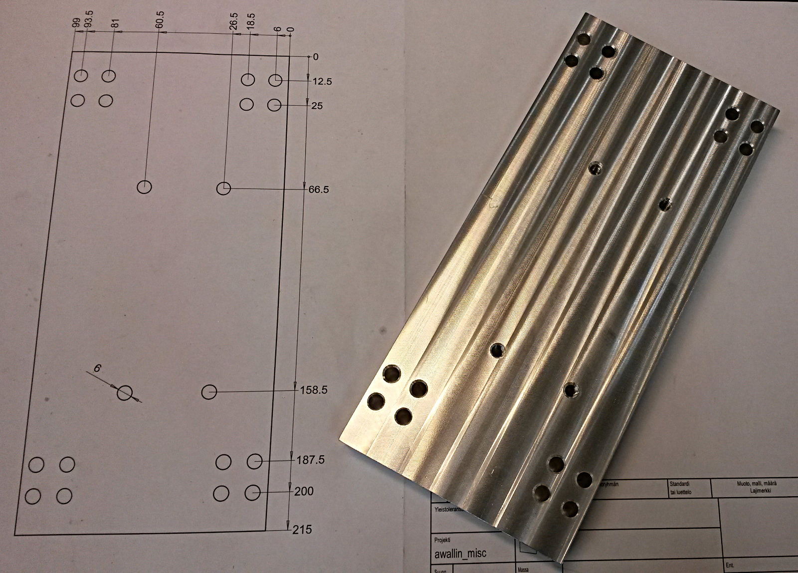
Riser Block
I cranked out this 27mm high riser-block from a piece of 35x100 mm aluminium bar today.
The 6mm holes in the corners are for attaching the block to a standard breadboard or optical table that has M6 threads on a 25mm pitch. There are four holes in each corner in a 12.5-by-12.5mm square pattern. These allow attaching the block with 12.5mm 'resolution' both along X and Y.
The middle M6 tapped holes are for attaching to a translation stage. The stage is old with a weird 34x92mm bolt pattern.