I've put together the first version of a DC-bias amplifier used for applying four DC-voltages to the trim electrodes of an ion trap. The axial voltages required are low, and they are applied symmetrically as +Vz and -Vz. The transverse voltages (X and Y) however can be as high as 100 V. Two high-voltage op-amps PA340CC are used for the X and Y channels, while the -Z and +Z output voltages are produced by two OPA454 op-amps. The amplifier has three +/-10 V inputs (Vx, Vy, Vz), and produces four outputs designed to be 10*Vx, 10*Vy, -Vz, and +Vz.
The amplifier circuit itself is very simple with the two PA340CC's in non-inverting configuration with a gain of 10, and the two OPA454's in inverting configuration, connected in series, with a gain of 1. The bandwidth requirement is very low, and the load should be equivalent to an open circuit - hence high 100k output resistor and a cap producing a 16 Hz low-pass filter on the output
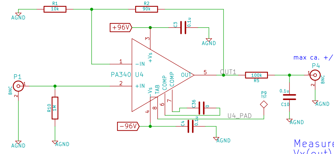
See full schematic as PDF: bias_amp_v0
The high-voltage DC-rails for the op-amps are produced by connecting four +/-24 V DC-to-DC converters in series. This allows powering the amplifier from a single +12VDC powersupply-brick, and in theory produces +/-48 V for the lower-voltage op-amps and +/-96 V for the high-voltage op-amps.
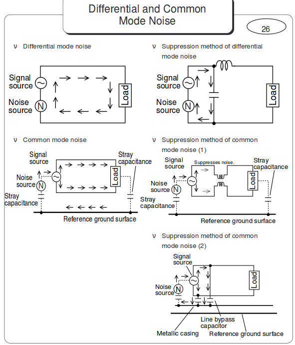
One issue with DC-to-DC converters is that they produce both differential and common-mode noise on the output. Conventional filter-caps or Pi-filtering removes the differential noise but does nothing to the common-mode noise. A common mode choke and/or filtering capacitors across the isolation-barrier to the input-side ground are required to remove the common-mode noise. Here's a picture from a Murata app-note that explains the idea:
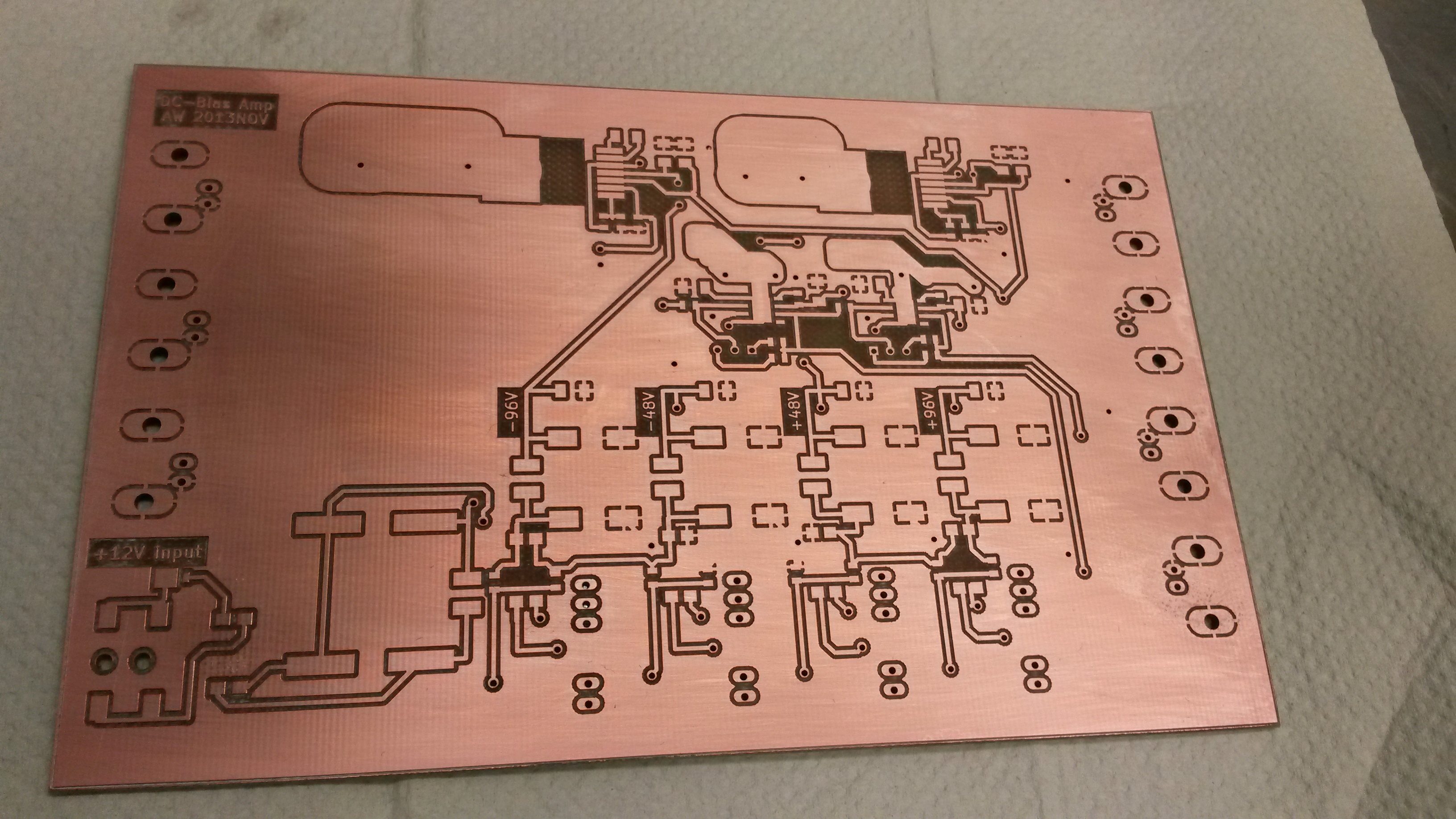
The components fit comfortably on a 100mm by 160mm PCB like this:
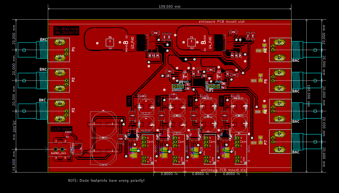
Only top Cu-layer shown. Why doesn't Kicad have built-in PDF export for the PCB-editor (like in the schematic-editor)?
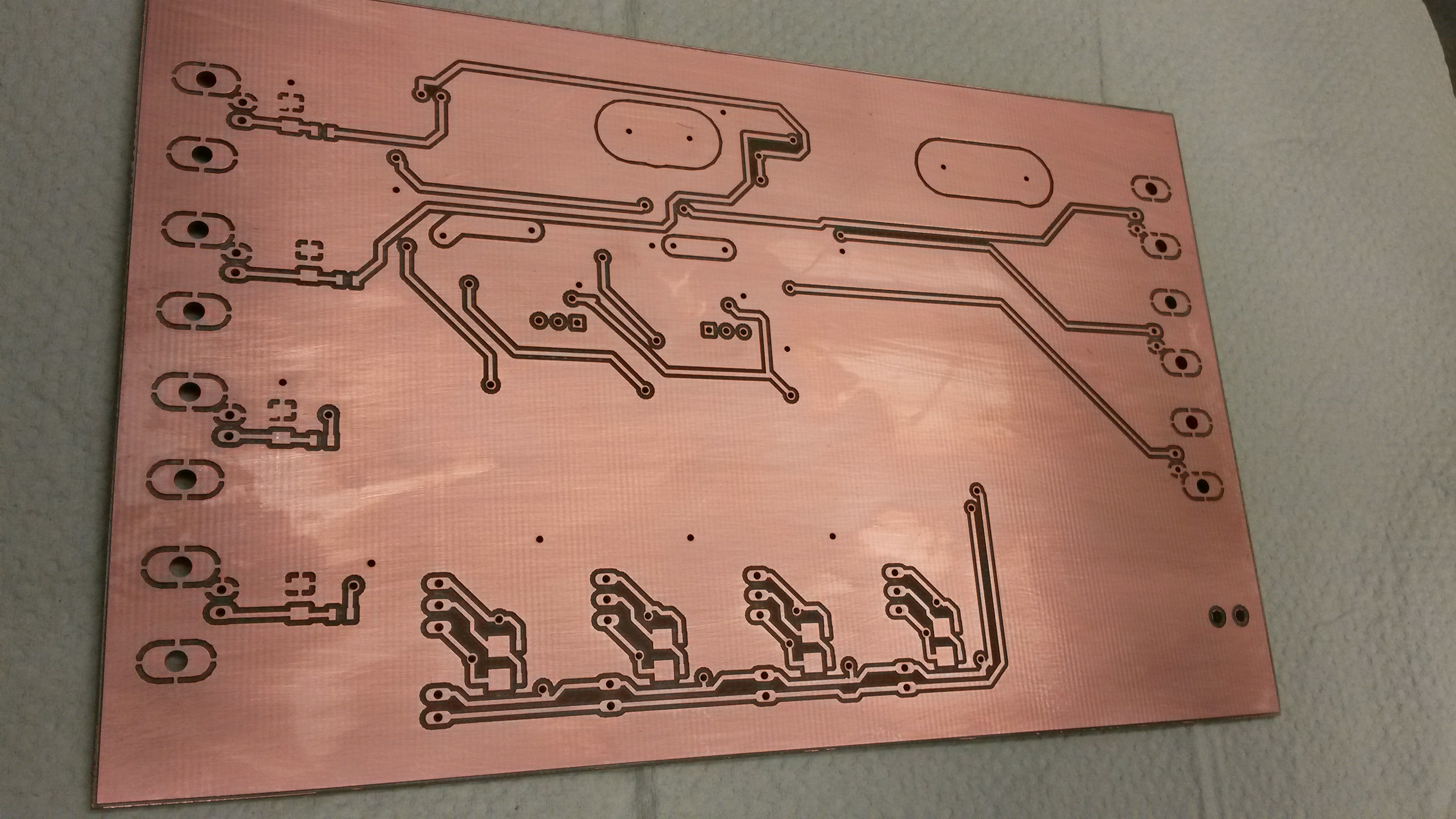
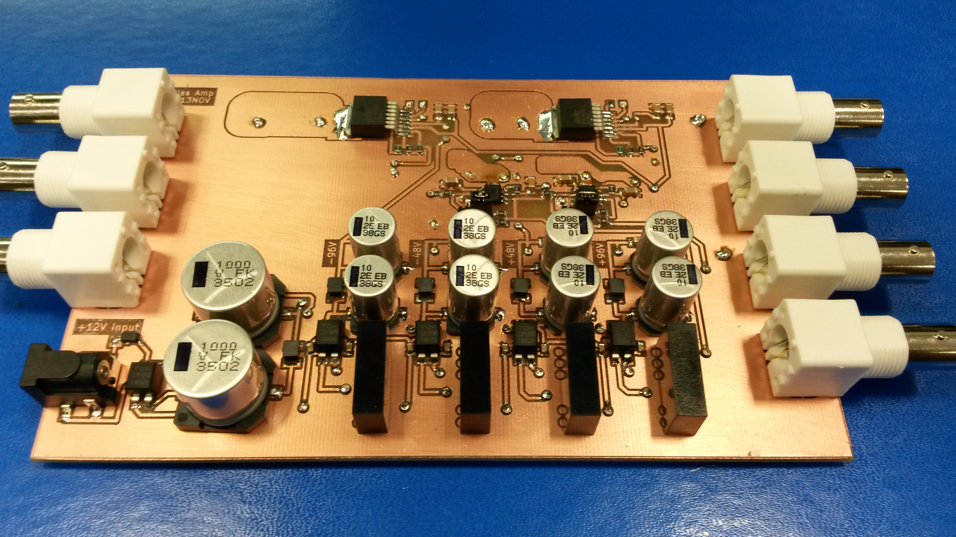
Gerber and Excellon files from Kicad worked without problems with CircuitCAM for producing toolpaths for BoardMaster that runs our LPKF PCB mill. The PCB after milling, rubbed with steel-wool, cleaned with isopropanol, and then coated with PRF202.
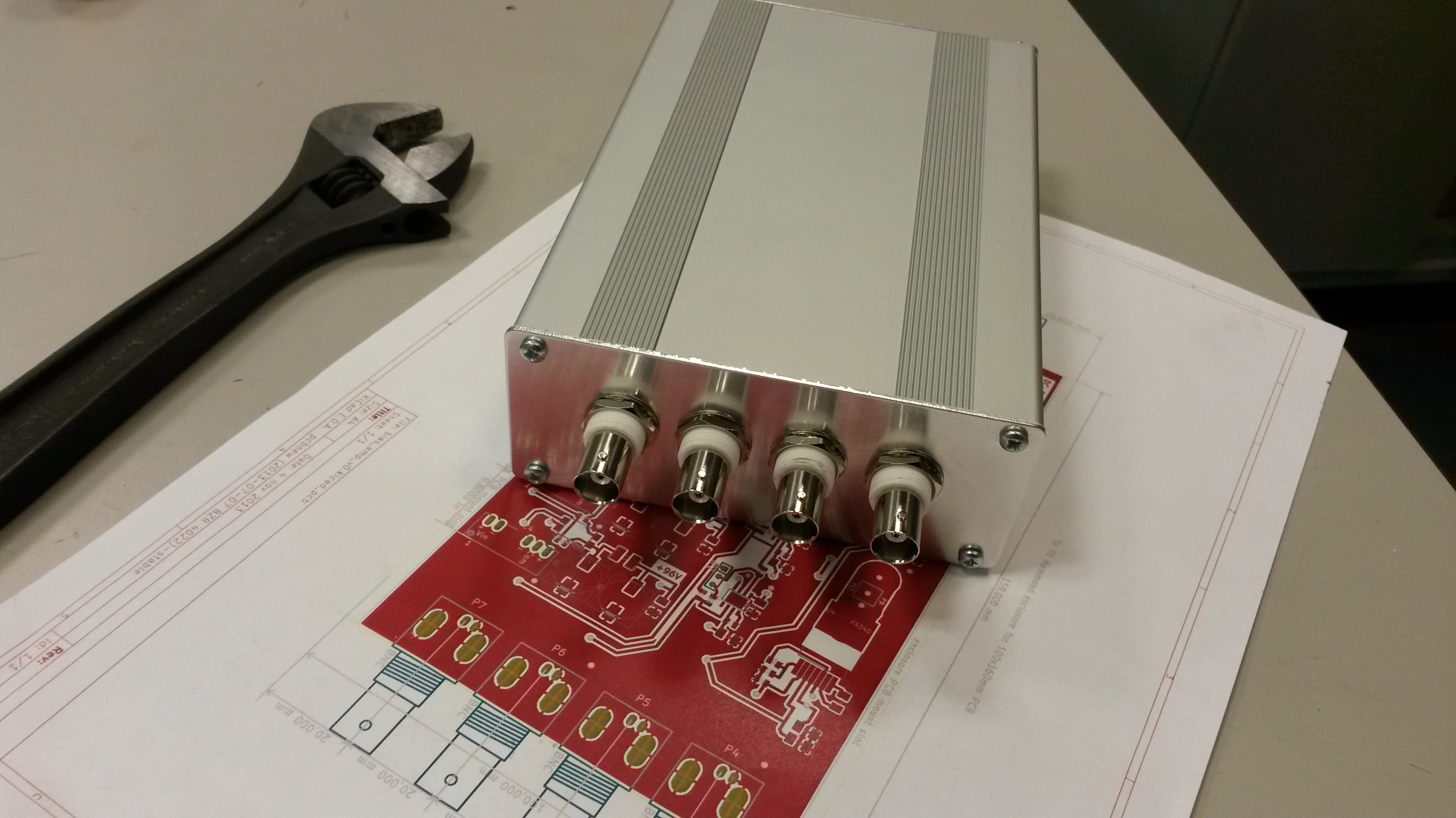
Components soldered, and board fit into an enclosure (Multicomp MCRECS160):
When powered up the DC-rails measured slightly lower voltages than expected. I got -89V, -44V, +44V, and +89V. The no-load input current was surprisingly high at 190mA. The dc-to-dc converters have a no-load spec of 20mA, so this explains about half of the measured current. The op-amps have a quiescent current of 3.2 mA @ +/48V for OPA454 and 2.2 mA @ +/-96V for PA340. So the 'middle' DC-to-DC converters that power all four op-amps should have 2*(3.2+2.2)= 10.8mA load at 48V and the 'side' converters only 2*3.2=6.4mA at 48V. That's 17.2 mA at 48V together, which should correspond to 84 mA at 12V if we trust the 82% efficiency number from the datasheet. So we can explain 80mA as no-load current and 84 mA from the quiescent current of the op-amps. That's 164 mA together, which is about 85% of the 190mA number shown by the powersupply. If my reasoning here is way off please comment below!
Initial measurements shows that the outputs behave roughly as designed. The high-voltage outputs max out at about +/- 85 V. Note that the 10 MOhm input of a DMM measures only 99% of the actual output voltage, due to the high 100k output impedance of the amplifier.
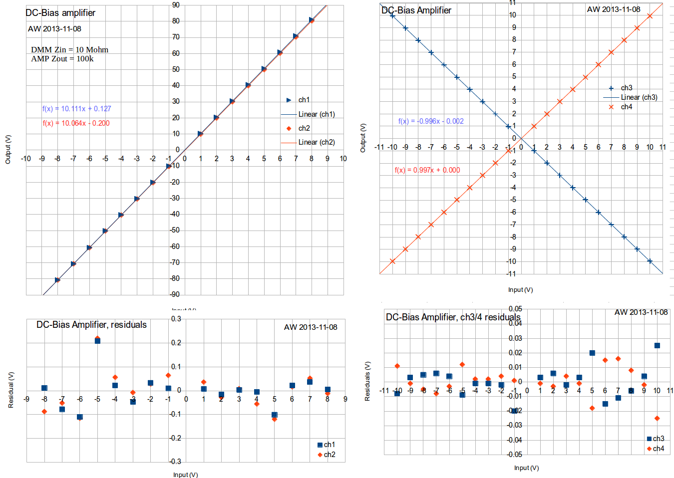
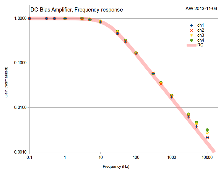
The frequency response is completely dominated by the 16 Hz low-pass RC-filter on the output, although the op-amps have unity-gain bandwidths of ~10 and ~2 MHz.
Notes and comments:
- This was the first board I designed with Kicad. It works rather well, and new enhancements are already on the way. The export of a netlist from the schematic-editor to the PCB-editor could be a bit smoother, and the footprint assignment should probably be done in the schematic-editor and the current CvPCB footprint-assignment bypassed.
- I used quite conservative design rules(mils): clearance 16, track 25, via 55, via drl 35. This seems to work quite well. The clearance could be reduced down towards 8 mils which is the minimum isolation clearance the PCB-mill can produce. Kicad automatically enforces clearance and via design rules interactively while routing the tracks - this is probably good once you get used to it.
- I messed up the polarity of the diode footprints - should be fixed if a second version is built.
- Linear regulators could be added on the DC-rails, after the pi-filters. Or perhaps a shunt regulator on the high-voltage rails.
- With no load the op-amps don't seem to heat up. So the heatsink copper areas may not be required.
- The BNC-footprint "BNC_Socket_TYCO-AMP_LargePads_RevA" has a quite large drill-spec for the mounting holes, could be reduced from 2.2mm to 2.1 or 2.0mm. The signal pin holes are also quite close to the large mounting holes. they could be moved further away by maybe 0.5 mm.
- I used kapton tape on the sides of the board, to insulate AGND from the aluminium case. Not sure what voltage the case should be at( +12V input ground?).
Footprint association in schematic editor:
https://www.youtube.com/watch?v=cD5CfHGre-g
another known good dc2dc and filter combination:
dc2dc: 12V to +/- 15V traco power, tes 2N-1223, Farnell 1007060
inductor: 3.3uH farnell 9621539
caps on input pi-filter: 10uF
30R resistor across inductor (adds damping, prevents ringing?)
common-mode choke: 2x200Z, Farnell 9621270
caps on output pi-filter: 1uF
thanks for this post. I googled many and found your post. currently I am using the same chip PA340 with +320V/-12.1V power. I know you used split lower rails. my problem is the PA340 got hotter and hotter. I simulated and it showed 820mW with no load. however it must be way beyond that. Could you tell me your light load power consumption of PA340 with 170V rail? did you feel the chip hot? or did you use forced air cooling? I doubted because you even didn't put a heatsink on...yours must be very cool with light load.....thanks.
Hi Lee, we have used this circuit only to provide DC-voltages to electrodes, i.e. pieces of wire, inside a vacuum chamber. There is no current flowing whatsoever, so the power-dissipation is very close to zero.
With 1W or more dissipation you should either provide a large ground-plane, possibly on both sides of the PCB with a lot of vias between the planes, or an additional heatsink that is soldered to the ground-plane (or device itself?).
Anders