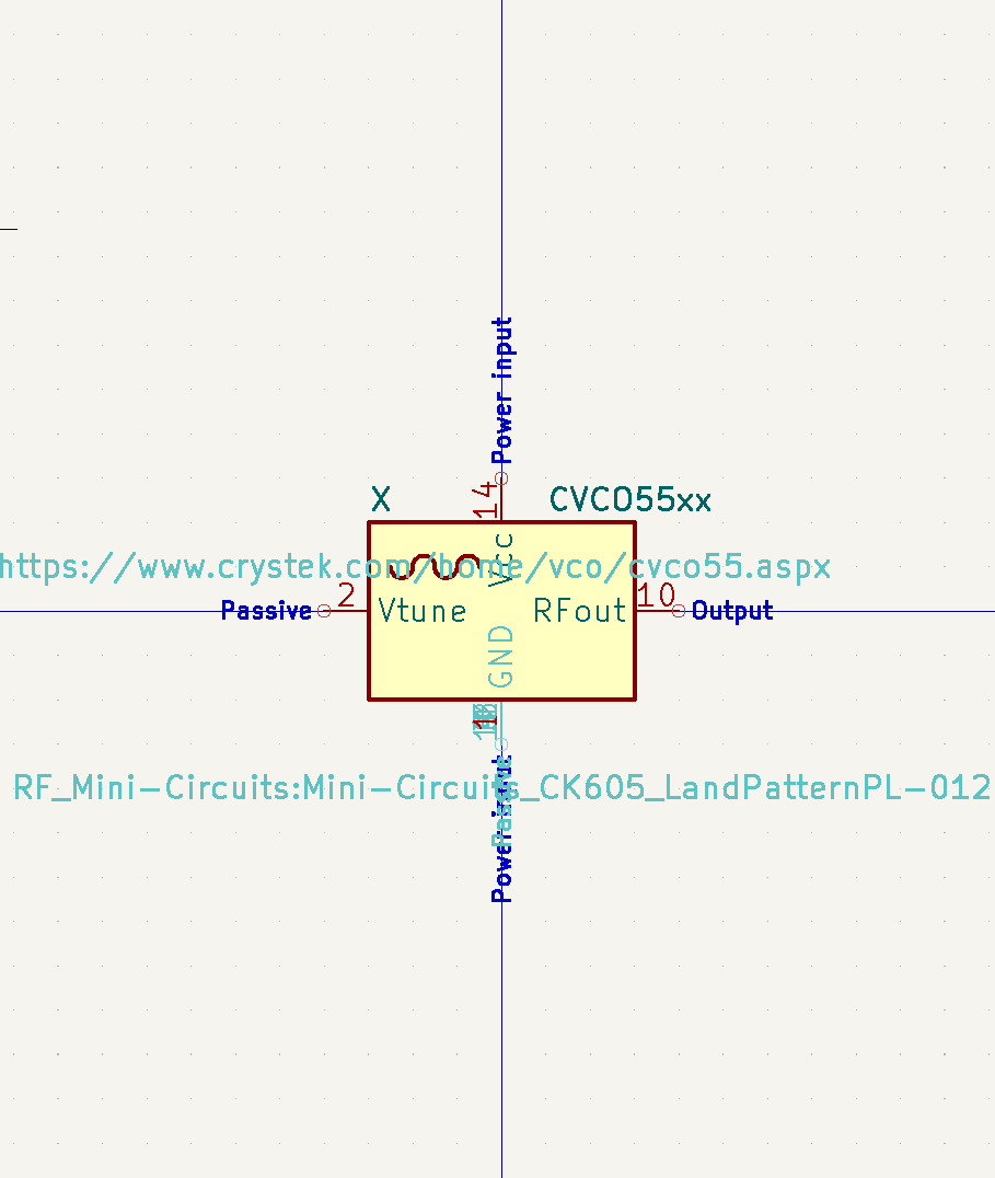
Crystek CVCO55 VCO
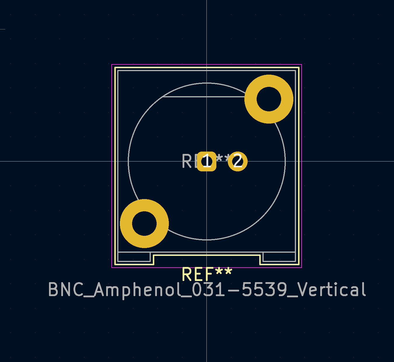
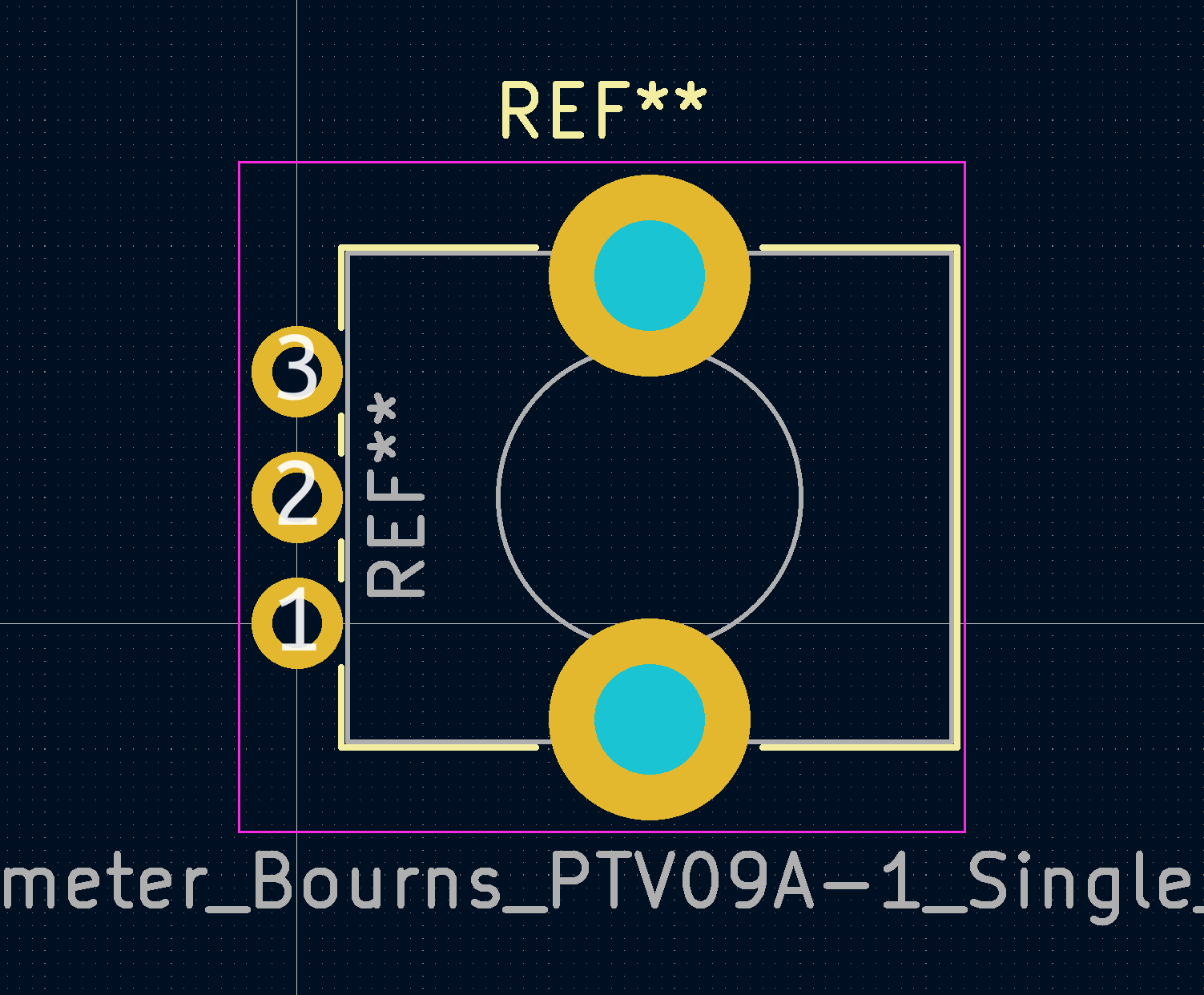
This footprint had too small mounting holes, and the potentiometer-shaft in the wrong place. https://gitlab.com/kicad/libraries/kicad-footprints/-/merge_requests/2991
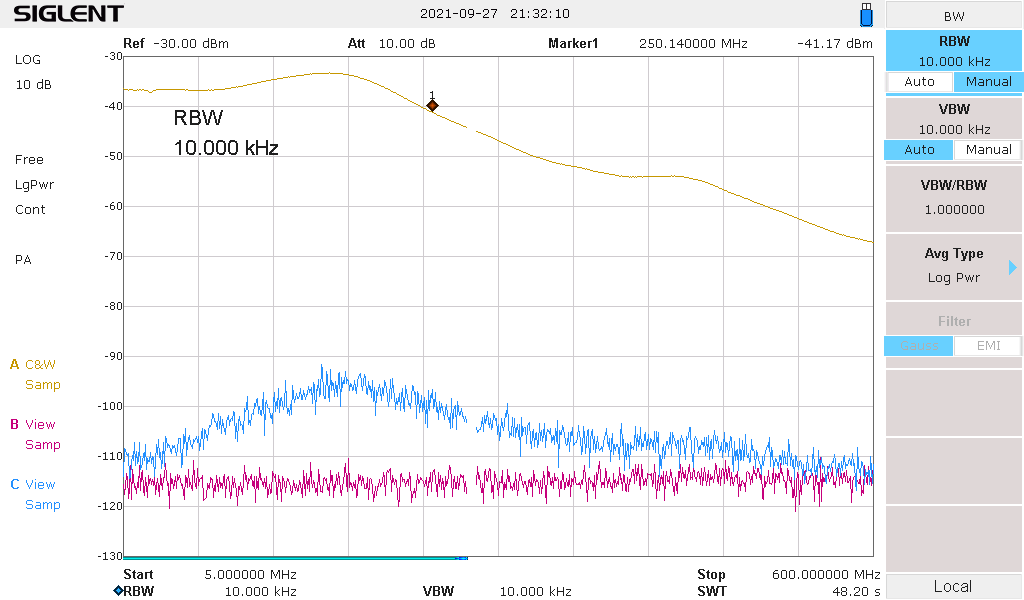
Here's anoter one-inch-photodetector with a Fermionics FD80FC photodiode and 5k1 transimpedance. Bandwidth around 250 MHz. Predicted dark noise and frequency response with TIASim. The Fermionics diode has a capacitance of only 0.4 pF (80 um diameter active area), giving slightly better bandwidth than a Thorlabs FGA01FC (2 pF capacitance, 120 um diameter active area).
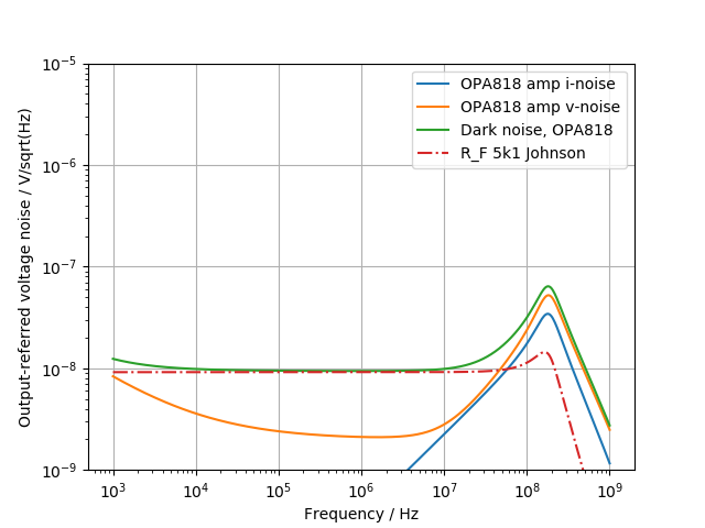
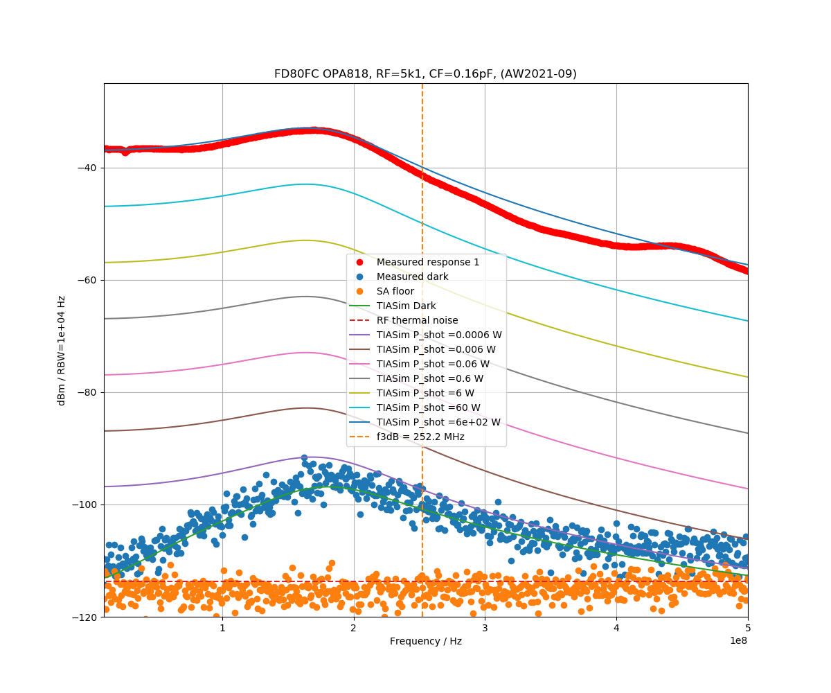
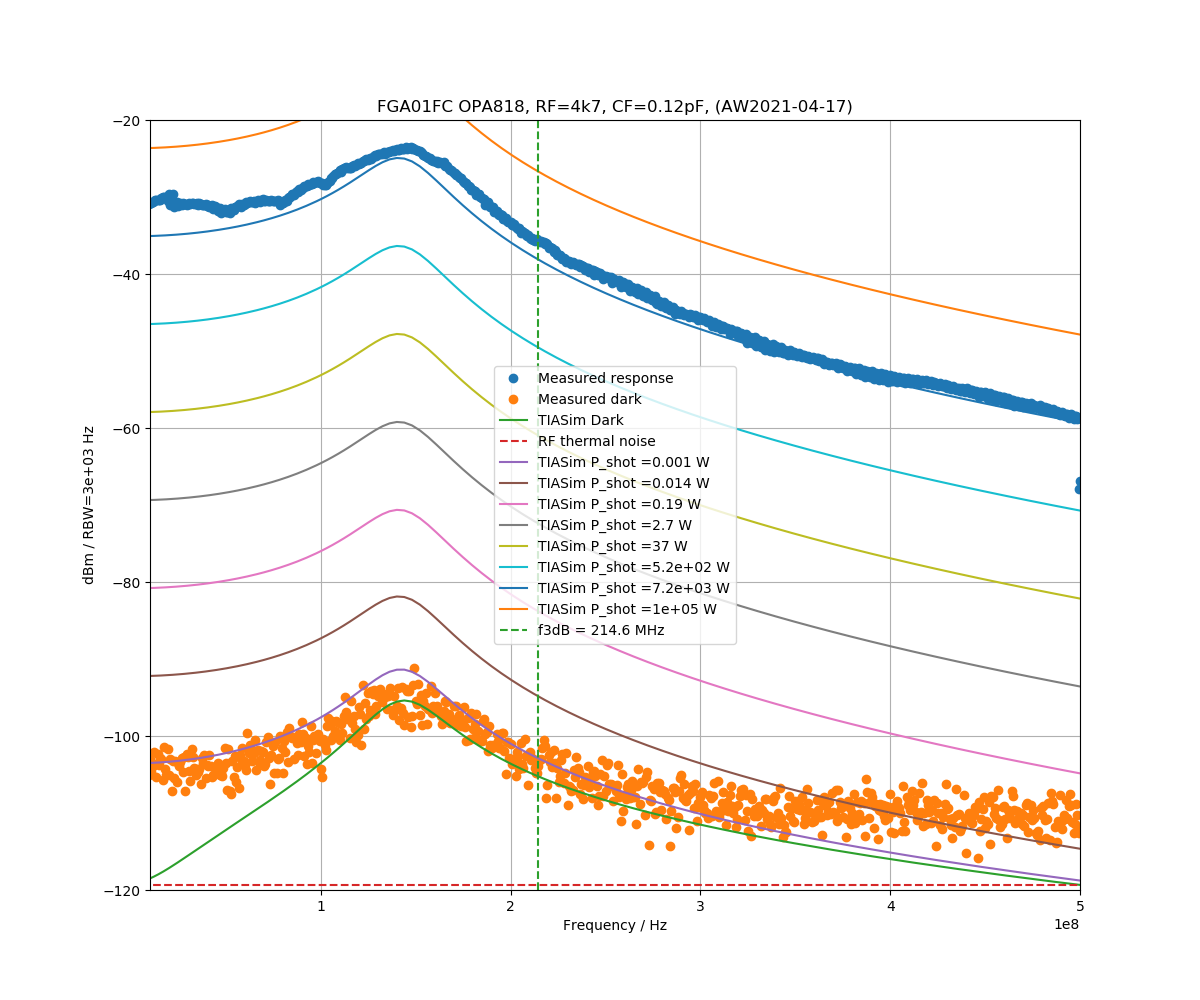
Transimpedance model: TIASim
Previous similar designs:
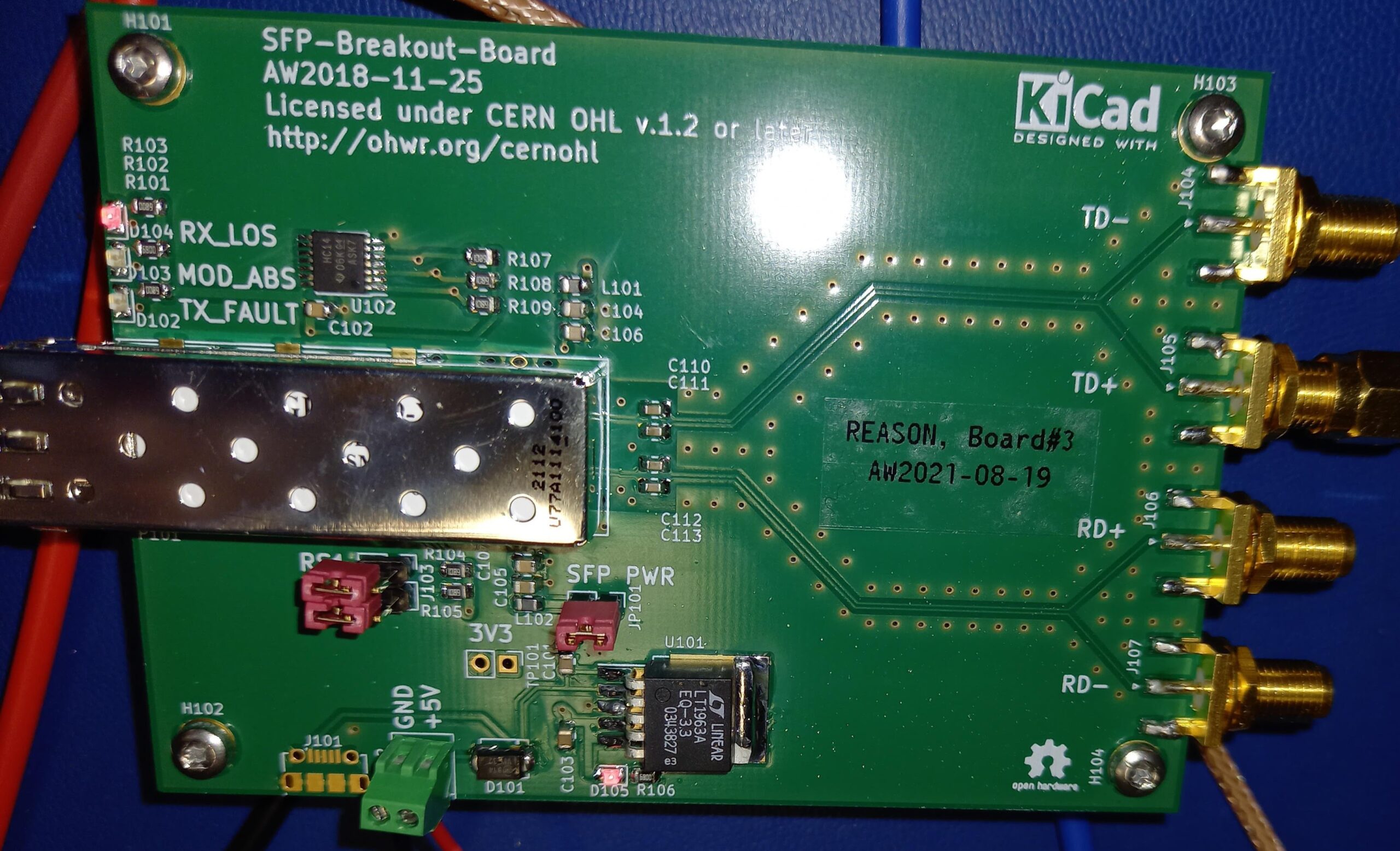
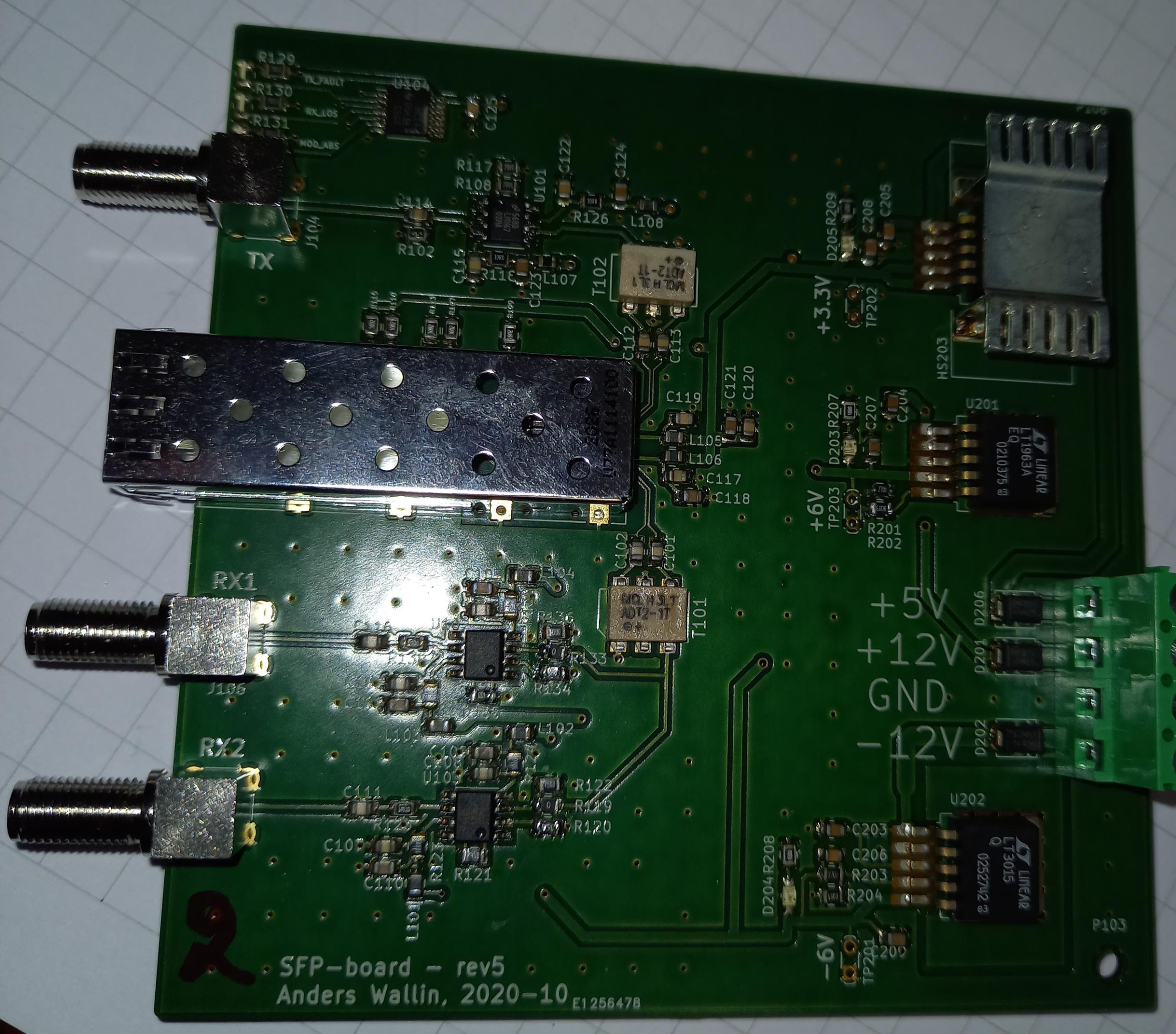
I made a new batch of the SFP Breakout Board.
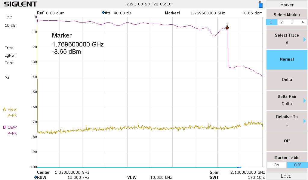
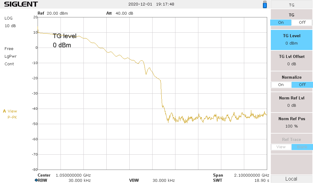
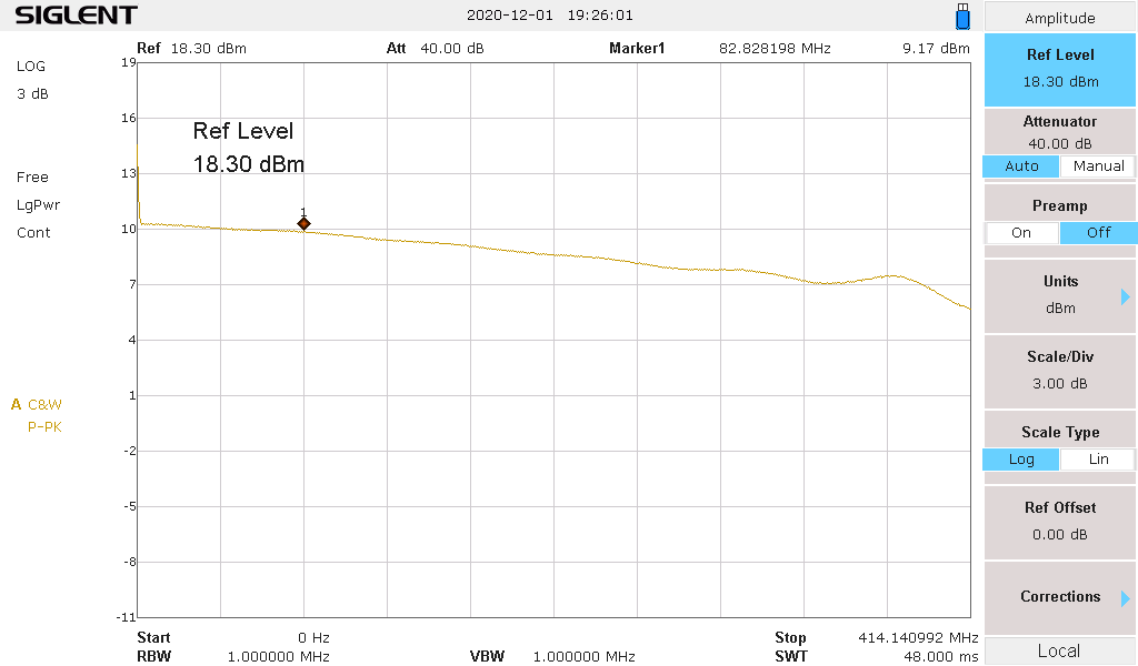
With a 1 Gbit/s SFP transciever the bandwidth when transmitting from the TX port of one board to the RX port of another board seems to be almost 1.8 GHz.
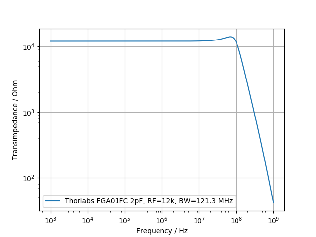
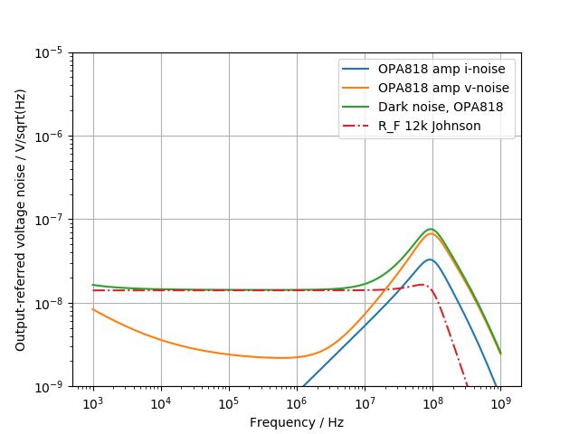
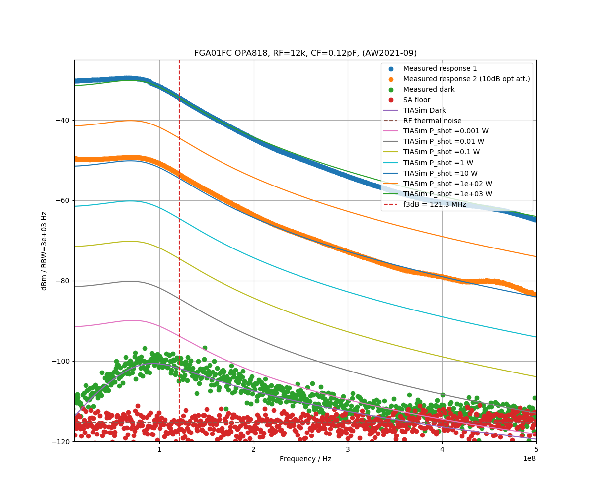
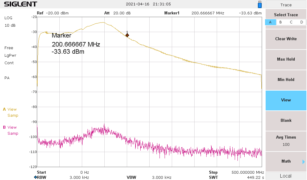
Here's another one-inch-photodetector using OPA818 with a 2pF@5V InGaAs fiber-coupled photodiode FGA01FC. With a transimpedance gain of 4k7 Ohms the bandwidth is just over 200 MHz. A TIASim model predicts the dark-noise and response reasonably well with a parasitic capacitance (over RF) adjusted to ca 0.12 pF. The spectrum-analyzer settings weren't ideal for looking at the dark-noise which should go down to the thermal-noise of the 4k7 resistor (dashed line) - but here the instrument noise-floor prevents us from seeing that.
Update: first production batch being tested in the lab 2020-12-17:
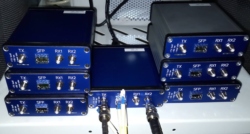
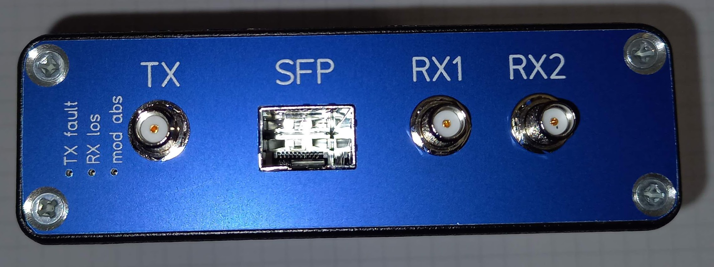
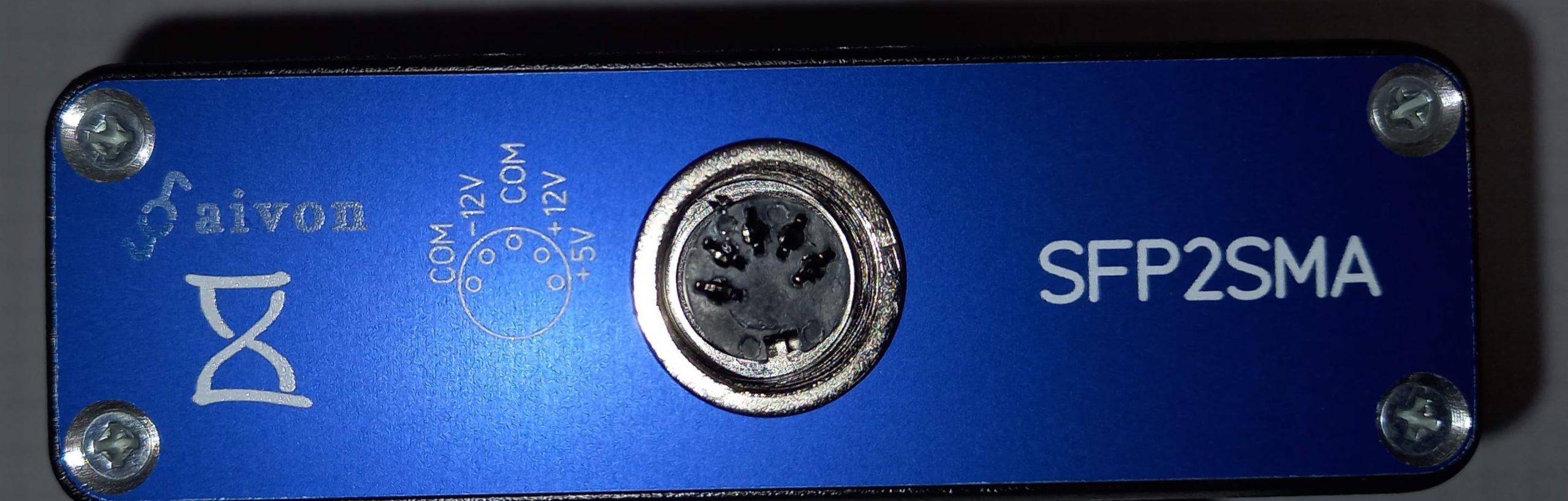
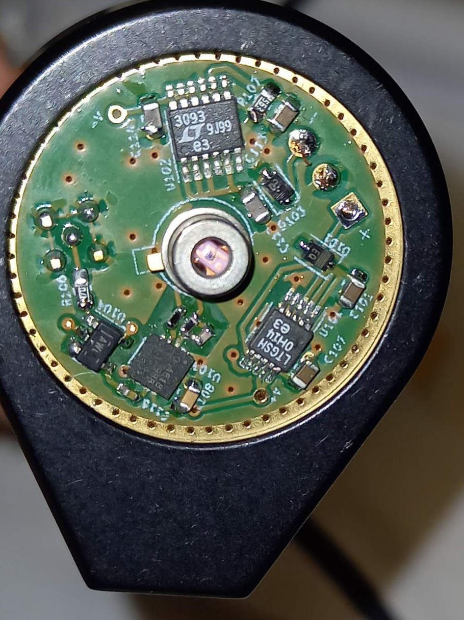
By popular demand, I've worked with Aivon to put my simple 'SFP2SMA' board (https://github.com/aewallin/SFP2SMA_2018.03) in a box, using an external Meanwell (+12V, -12V, +5V) PSU with a 5-pin DIN8 plug (model GP25A13D-R1B, Digikey 1866-1826-ND). The board can be used for simple frequency-transfer experiments together with almost any SFP-transciever. The TX SMA-connector is an input, and applies the waveform to the TX-pins of the SPF, producing modulated optical output. The dual RX SMA-connectors are driven by the SFP RX-pins, with some gain applied to produce around +10 dBm square-wave into a 50R load.
The front panel has three SFP status-LEDs: TX-fault (I've never seen this, but apparently the SFP should report if the TX-laser fails), RX LOS (loss of signal, active if you unplug the fiber), and mod_abs (module absent, active if no SFP is plugged)
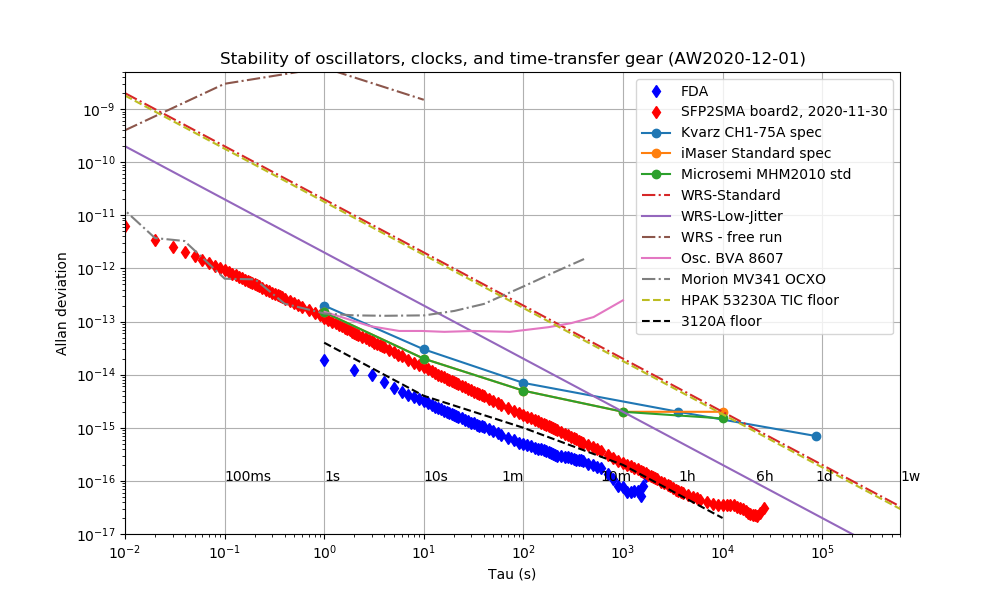
After some adjustments to gains and component values the frequency-response is flat within 3 dB out to ca 400 MHz, and the ADEV looks reasonable at ca 1e-13/tau(s) (red datapoints in the plot below). These measurements were done with a CWDM SFP and a 2m single-mode loopback-fiber.
The box is a Hammond 1455L1201 (120 mm x 103 mm x 31 mm), with custom front and back panels.
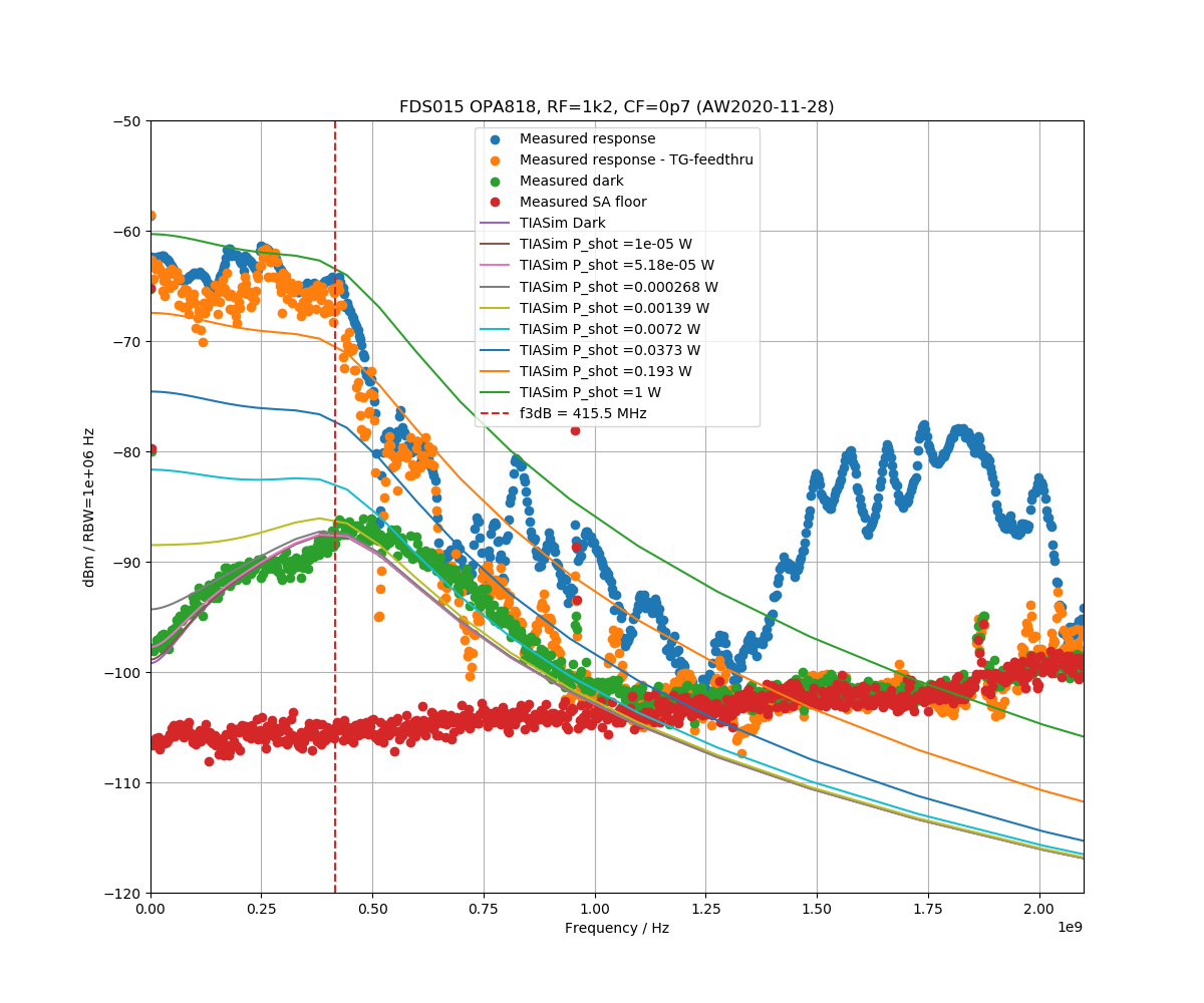
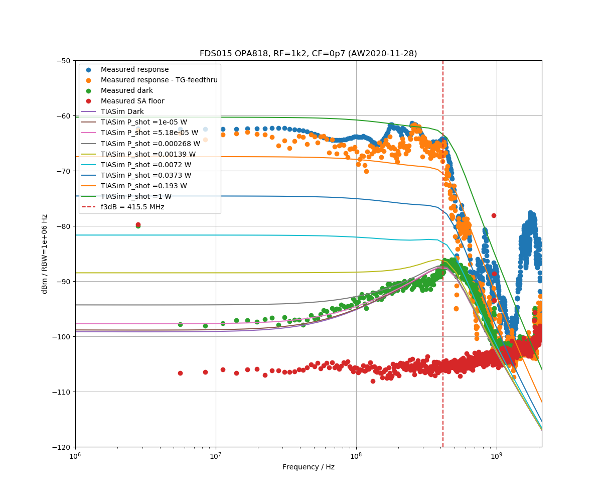
After a number of failed attempts (with HMC799, OPA859), here is a reasonably fast One Inch Photodetector using OPA818, a FDS015 photodiode, and 1.2 kOhm transimpedance. Bandwidth is above 400 MHz, with the dark-noise and frequency-response in reasonable agreement with TIASim predictions.
With the detector blocked there's quite a lot of electrical feed-through with just the spectrum-analyzer TG-output on (see blue data points, especially above 1 GHz). I tried to correct for this roughly, shown as the orange data points.