THS3491 test

Update: see also http://www.ke5fx.com/ths3491.htm

Update: phase-noise with Rg=Rf=4k7. 

THS3491 looks like a good op-amp for frequency distribution amplifiers.

I tried it with a slightly modified FDA-design. With 200R feedback/gain-resistors it self-oscillates, but with 1k resistors (976R suggested in datasheet) it is stable. However I see 16dB of gain-peaking!

Using +/-13V3 supply-rails it does drive a 20Vpp sine-wave-ish looking waveform into a 1 MOhm load.

Phase-noise TBD, if and when the gain-peaking is resolved.

Note stylish extra pins on PCB to ground pin1...

Distribution Amp - S/N 16

Update2: Here's the 14-hour data together with a 14-hour noise-floor run. The ADEV and TDEV results are more or less instrument-limited. Only for phase-noise above 100Hz offset is the instrument floor significantly below the result for the distribution amplifier.

Update: Here's a 14 hour run of the residual phase noise, ADEV, and TDEV, as measured through the frequency distribution amplifier. Instrument is a Microsemi 3120A phase-meter.

Aivon has now produced around 16 of these distribution amplifiers.

There's a new op-amp which might be interesting to try for the FDA board: THS3491. It has a grounded pad under the op-amp, so we need a new EP-variant of the PCB.

Frequency Distribution Amplifier 2017.01

1:8 frequency distribution amplifier based on LMH6702 and LMH6609 op-amps.

In particular the power-supply section using a common-mode choke, a Murata BNX025 filter, and low-noise regulators LT1963 and LT3015 seems to work quite well. I also used ferrites (2 kOhm @ 100 MHz) as well as an RC-filter on all supply pins. Perhaps overkill? Performance with the intended AC/DC brick is still to be verified.

Measurements around 10 MHz show a 1 dB compression at over 14 dBm and an IP3 of around 27 to 30 dBm. The gain extends beyond 100 MHz with some gain-peaking.

Some measurements of residual phase-noise with a 3120A phase-meter, at 10 MHz. My earlier distribution amplifier required shielding with aluminium foil as well as powering from a lead-acid battery to achieve a reasonably quiet phase-noise spectrum. These measurements were done with lab power-supplies for +/-12 V to the board and without any shielding.

Finally some measurements of gain vs. frequency with a Rigol spectrum analyzer.


Distribution Amplifier 2017.01

A new distribution amplifier design featuring a 1PPS pulse distribution amplifier (PDA) and a 5/10 MHz frequency distribution amplifier (FDA).

1U 150mm deep rack-enclosure from Schaeffer. Prototype PCBs without soldermask or silkscreen from Prinel. Both the FDA and PDA boards have 1:8 fan-out with 9 BNC (optionally SMA) connectors spaced 16mm apart. The boards fit comfortably side-by side on a 19" rack panel. Some funky BNC-cables with unusually large connectors may not fit side-by-side 16mm apart - a price to pay for the compact design. The plan is to use an +/-12 AC/DC brick power-supply (not shown) which fits in the back of the enclosure.

Detailed posts on the PDA and FDA boards to follow.

Ettus OctoClock distribution amplifier

I measured the phase-noise of an Ettus OctoClock distribution amplifier. These plots compare it to earlier measurements on an SRS FS710 and a Symmetricom 6502 as well as my own TADD-1 inspired AD8055 prototype.

OctoClock schematic here: http://files.ettus.com/schematics/octoclock/octoclock.pdf

10 MHz clock-distribution chip: http://www.ti.com/lit/ds/symlink/cdce18005.pdf

For time-nuts kind of stuff (H-masers!) the 10 MHz phase-noise doesn't look that great, and there is something funky going on in the AM noise!? The box is powered by a +6 VDC wall-wart PSU which is probably the cause of all those spikes...

The PPS-channels are based on 7404 hex-inverters and look OK. 200ps of skew is equivalent to 4 cm of trace-length (?) - which seems like a lot if there was an effort to minimize it... For a 1 V/ns rise-time pulse 200ps is equivalent to 200mV of DC-offset in either the signal or the counter trigger-level which also seems like a lot?

Frequency Distribution Amplifier, v2 simulations

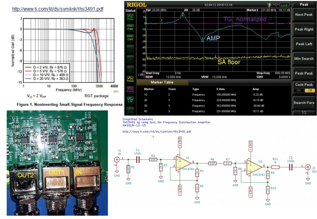
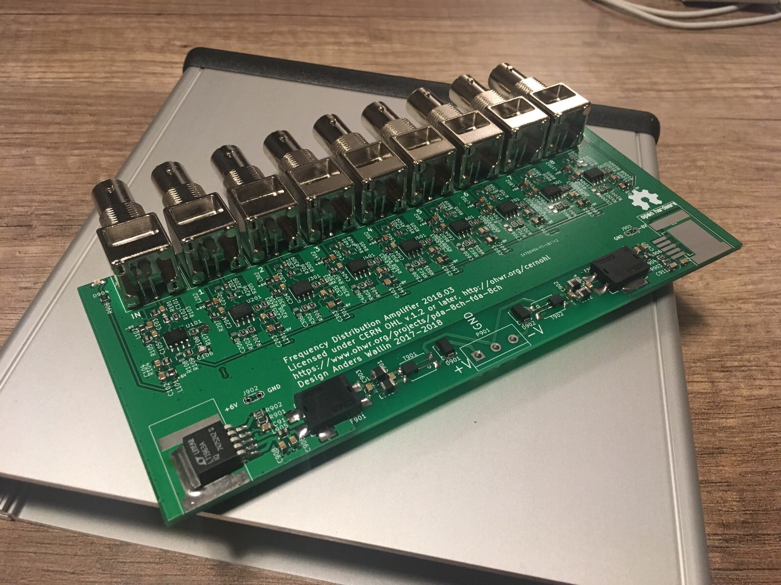
I wasn't entirely happy with my frequency distribution amplifier prototype measurements, so I decided to do some SPICE simulations.

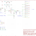
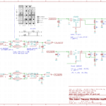
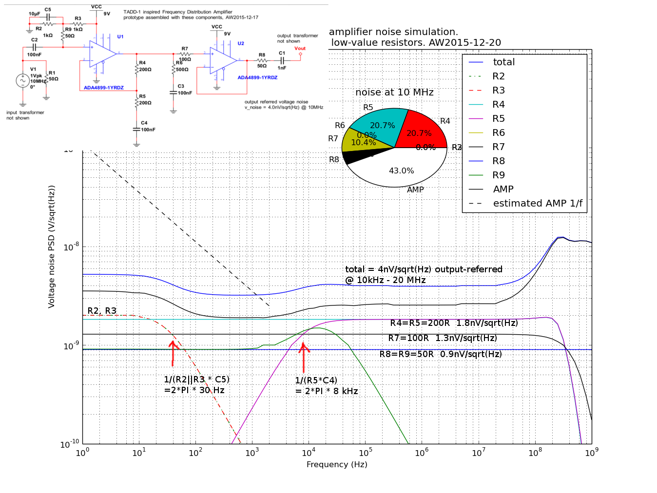
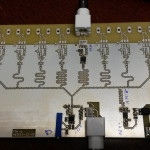
Here is a circuit close to the original TADD-1 design, configured for a voltage gain of 2, which when loaded with 50R corresponds to unity gain or 0 dB.

fda_noise_ad8055_with_comments

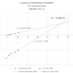
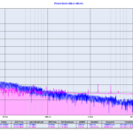
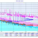
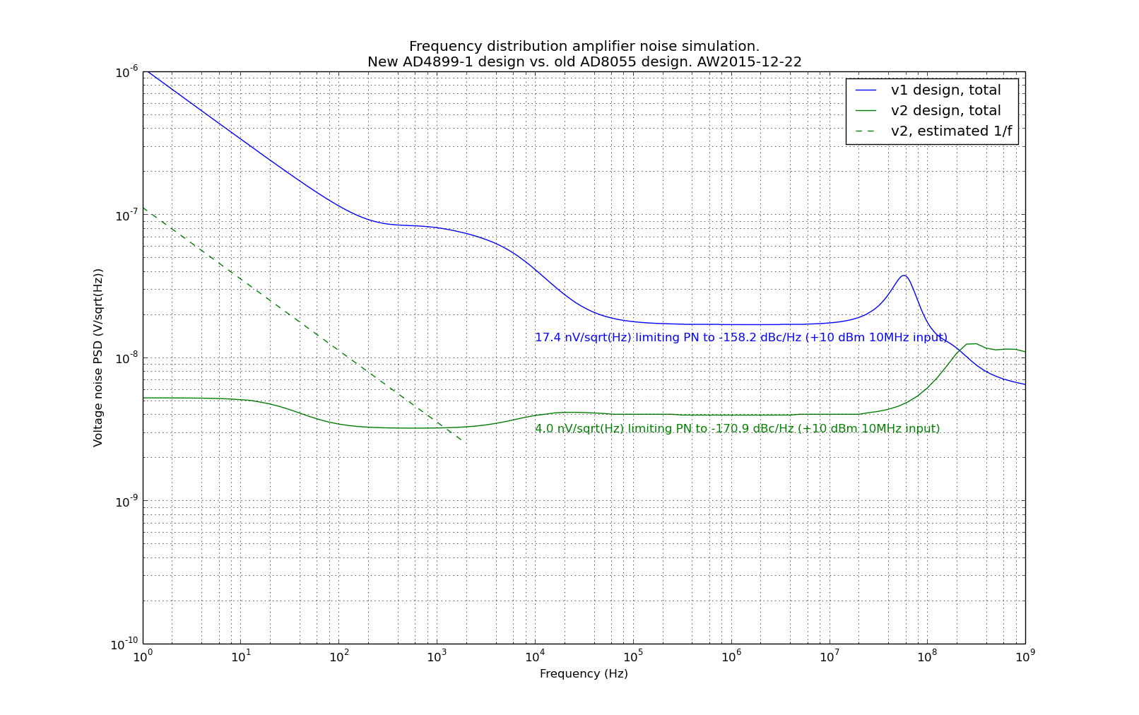
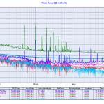
The main contribution to the noise floor at 10 MHz is by the AD8055 op-amp (roughly 3/4ths), with the gain-resistors R4 and R5 also contributing (roughly 1/4th). The simulation gives an output-referred noise-floor of 17.4 nV/sqrt(Hz) between around 100kHz and 20MHz. At low frequencies the 1/f noise of the op-amp dominates. The large 47k bias-resistors R2 and R3 are not bypassed/filtered in this design and they contribute significantly at low frequencies.

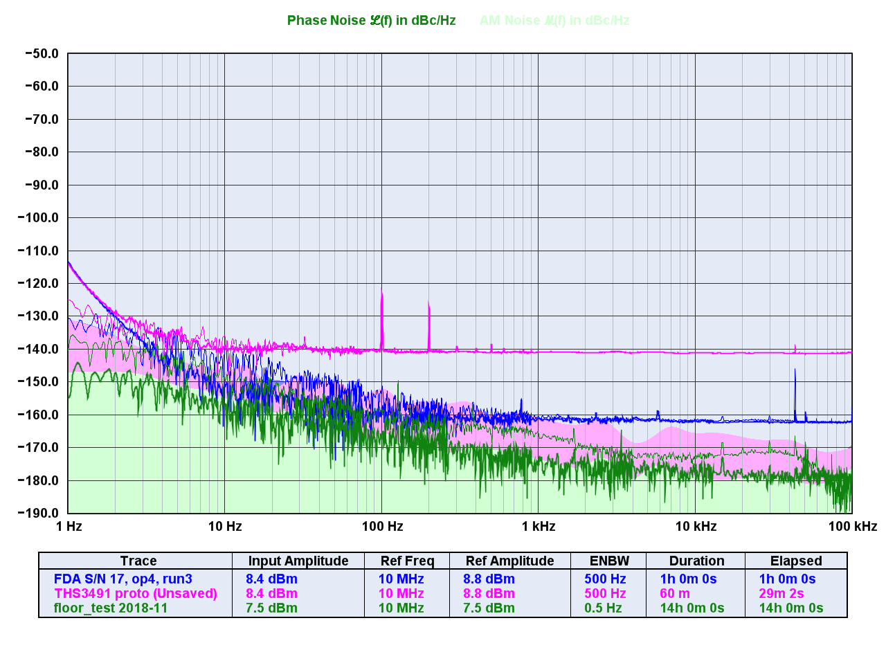
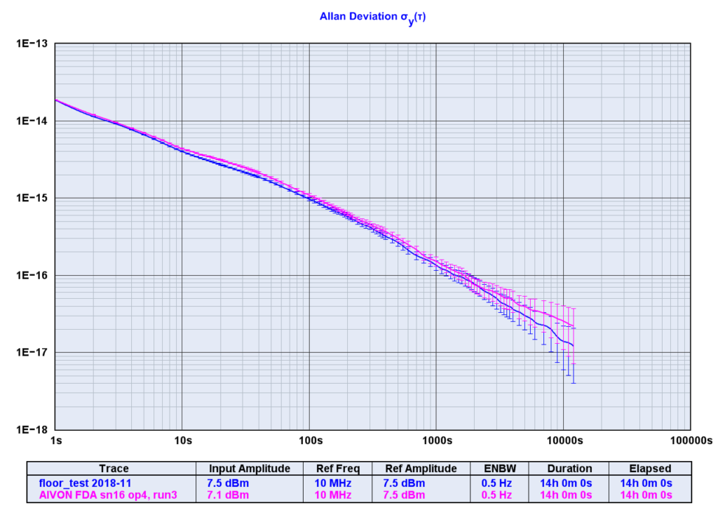
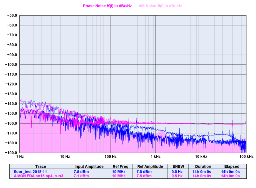
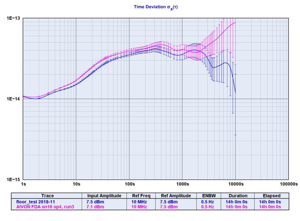
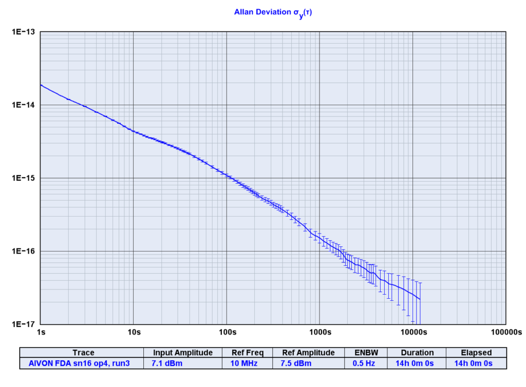
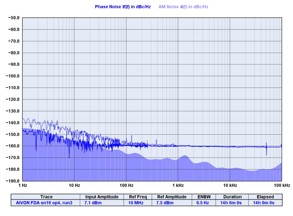
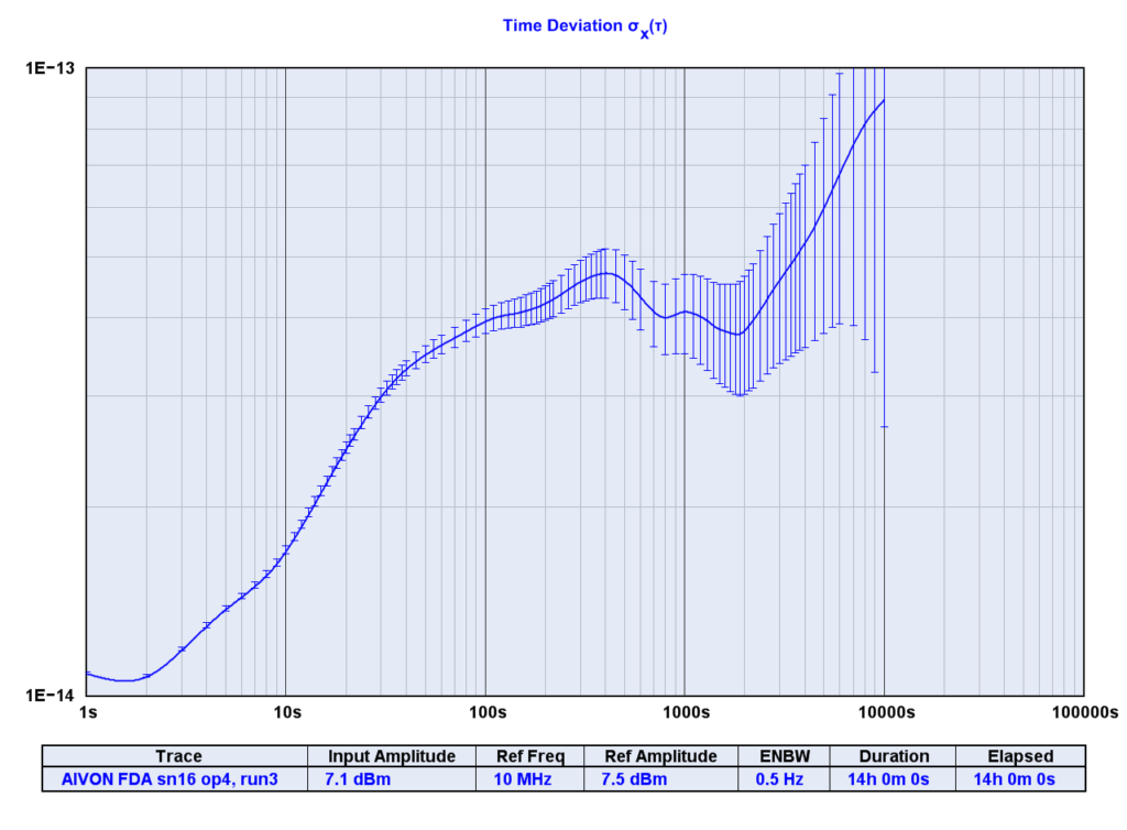
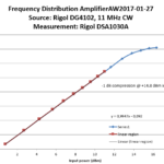
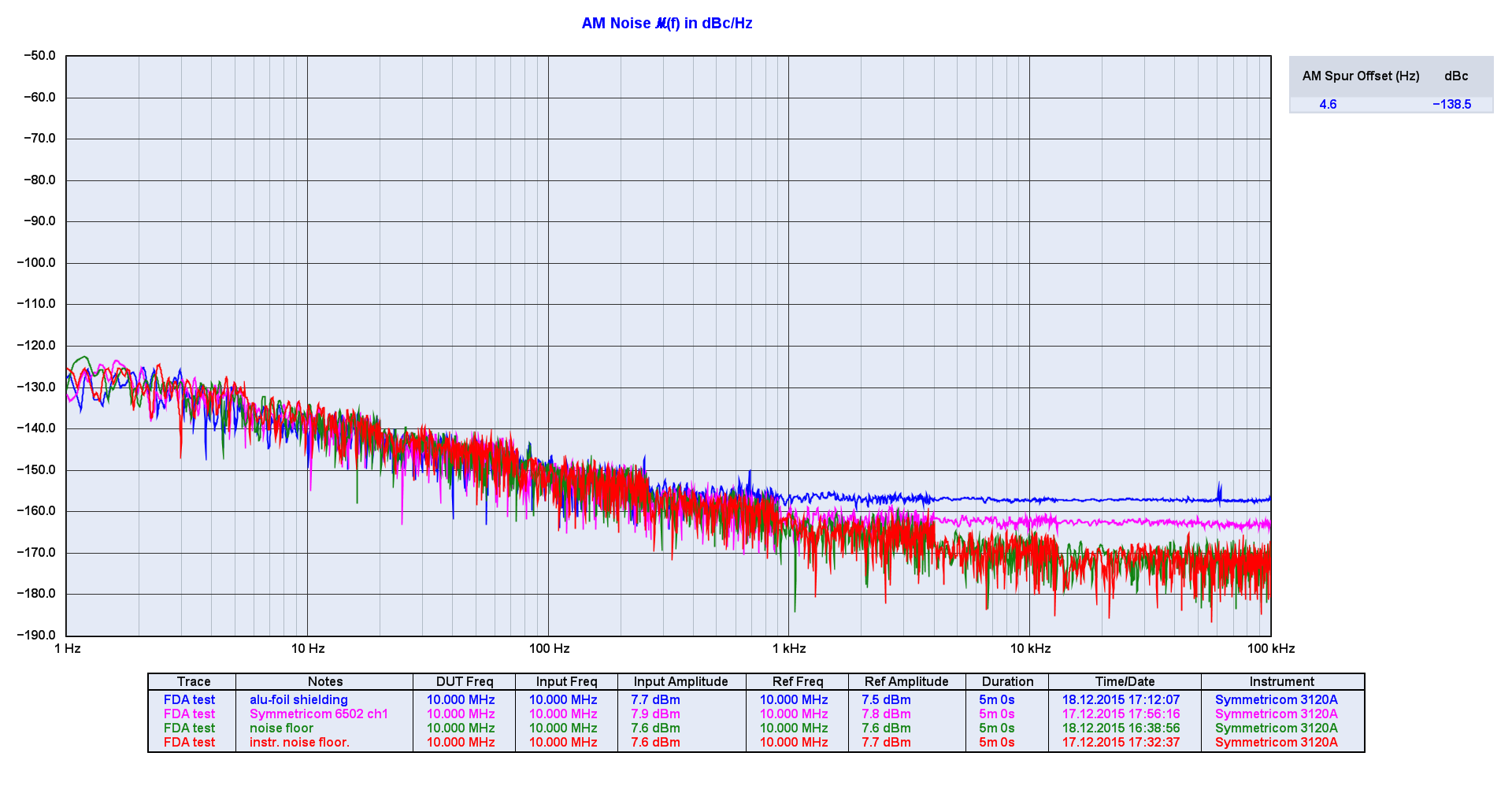
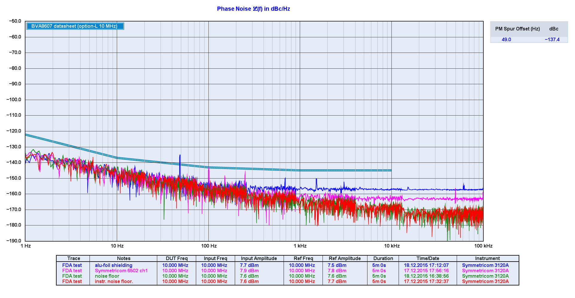
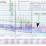
17.4nV/sqrt(Hz) is -142 dBm/Hz. This is a one-sided spectrum so we subtract 3 dB to get a single-sideband number, and then another 3 dB since noise is divided equally into AM and PN. This gives a best-case PN of -148 dBc/Hz for a 0 dB input/output power. In my measurements I got about -157 dBc/Hz with +7 dBm output.

fda_noise_opamp

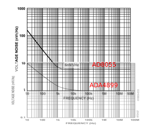
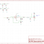
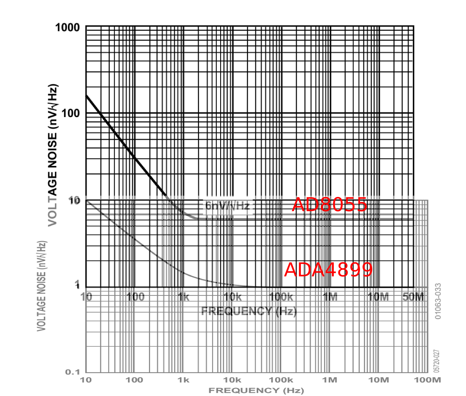
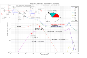
The v2 design uses the ADA4899-1 op-amp instead of the AD8055. This improves the op-amp input voltage noise floor from 6 nV/sqrt(Hz) to 1 nV/sqrt(Hz)  while also reducing the near-DC voltage noise by more than ten-fold.

fda_noise_ada4899_with_comments

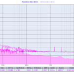
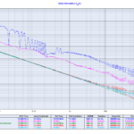
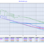
The simulation for the ADA4899-1 design shows an output-referred noise floor of 4 nV/sqrt(Hz) from 10 kHz to 20 MHz. This corresponds to about -155 dBm/Hz, a 12.7 dB improvement over the original design. The SPICE model for the ADA4899-1 does not include 1/f noise so I have estimated it with a dashed line. I have tried to minimize the resistor noise with reduced resistance values for the gain-setting resistors R4, R5, and a bypassed (C5) 'T'-circuit for the DC-bias (R2, R3, R9).

The theoretical PN floor with 0 dBm signal is now -161 dBc/Hz (again 13 dB better than for the original design).

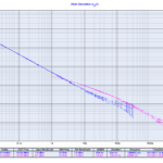
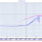
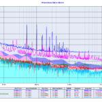
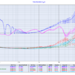
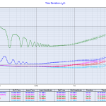
Here is a figure that compares the two simulations:

fda_noise_comparison

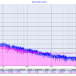
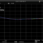
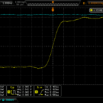
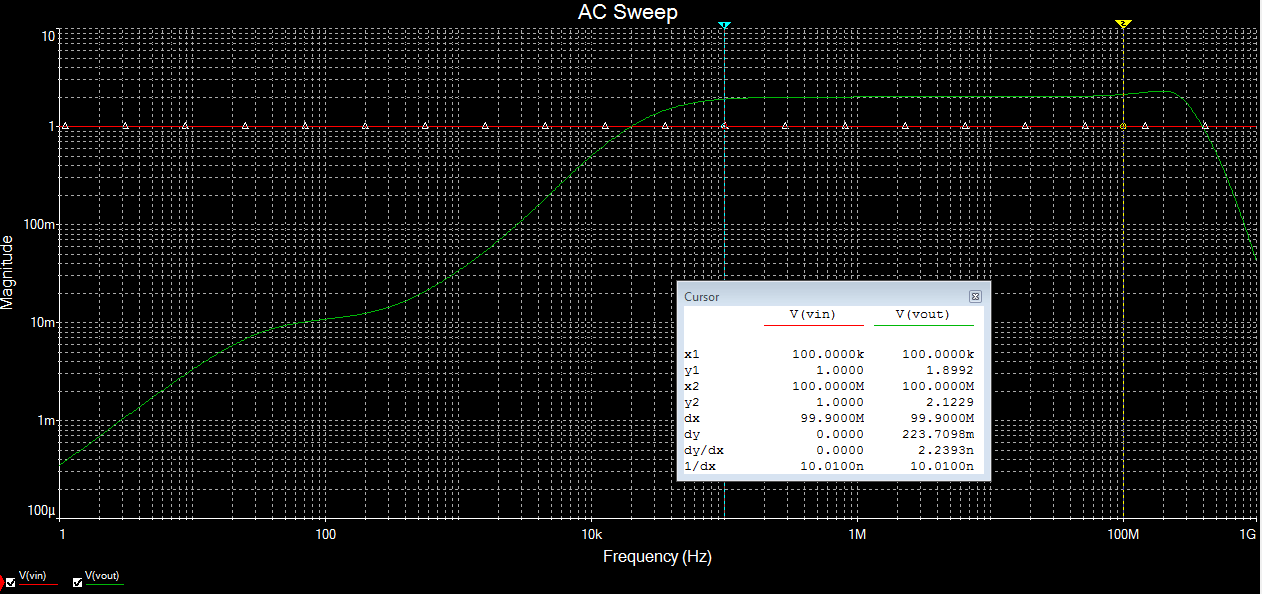
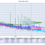
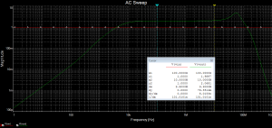
These figures show an AC sweep response for the SPICE simulations:

fda_v1_ac_sweep  fda_v2_ac_sweep

Further ideas and ToDo:

  • What is the limit for reducing values of R4 and R5? Power-dissipation, current-draw from the op-amp?
  • Reduce value of R7 - do we even need it.. (improves isolation between output stages?)
  • Replace R9 with an inductor - BUT it creates a resonance with C5 that needs to be damped - probably not worth it.
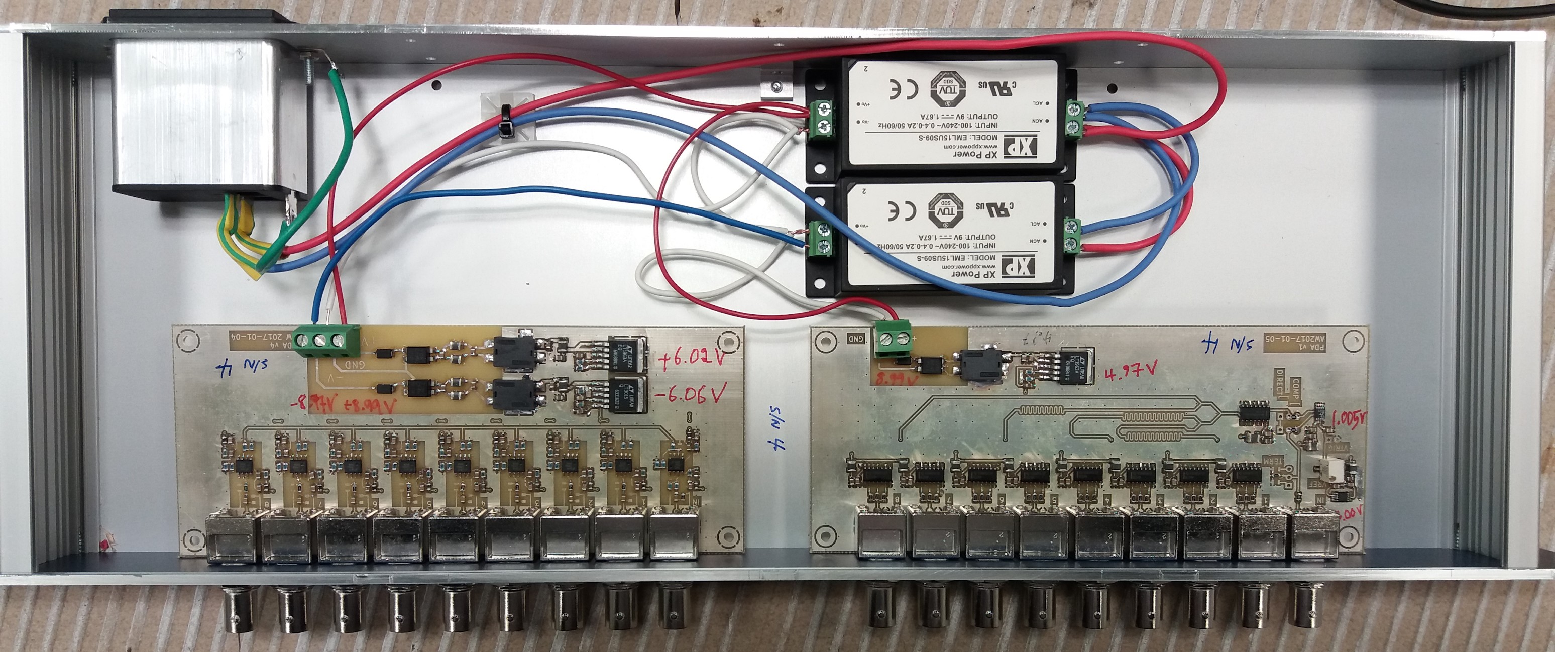
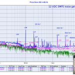
  • Improve on the powersupply schematic in the prototype. Spurs were big with a SMPS +12VDC supply.
  • Do PSRR simulations? Does that give different optimization goals for the DC-bias circuit?
  • Find an even better op-amp?
  • Where do we find a good SPICE model for ADA4899-1? The one I am using has a realistic AC gain response but unrealistic noise model near DC. There is an alternative on the analog.com website with realistic 1/f noise behaviour but infinite AC gain bandwidth!!??

Constructive comments are welcome!

Frequency Distribution Amplifier - first tests

Update 2015-12-18: Things improved quite a lot by simply wrapping the board in aluminium foil!
alufoil_and_battery_AMalufoil_and_battery

The amplifier phase noise floor is now at around -156 dBc/Hz while the 6502 is at -163 dBc/Hz. The AM noise numbers are similar.

Original post 2015-12-17: I put together a first prototype (only one output channel) of my TADD-1 inspired frequency distribution amplifier. Preliminary schematic here.

I compared the prototype board to two commercial distribution amplifiers: an SRS FS710 (quite awful) and a Symmetricom 6502 (very good). I also compared my new data with John Ackermann's measurements from 2007.

The new board showed ugly spurs at 50 Hz and harmonics using an el-cheapo wall-wart 12 VDC SMPS, so I also tried it with an "ultra-low noise DC-source" a.k.a 12 V lead-acid battery.