EEWeb.com will feature this site as the site-of-the-day tomorrow Thursday! Their circuit simulator at www.partsim.com looks interesting:
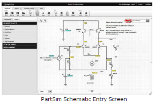
EEWeb.com will feature this site as the site-of-the-day tomorrow Thursday! Their circuit simulator at www.partsim.com looks interesting:
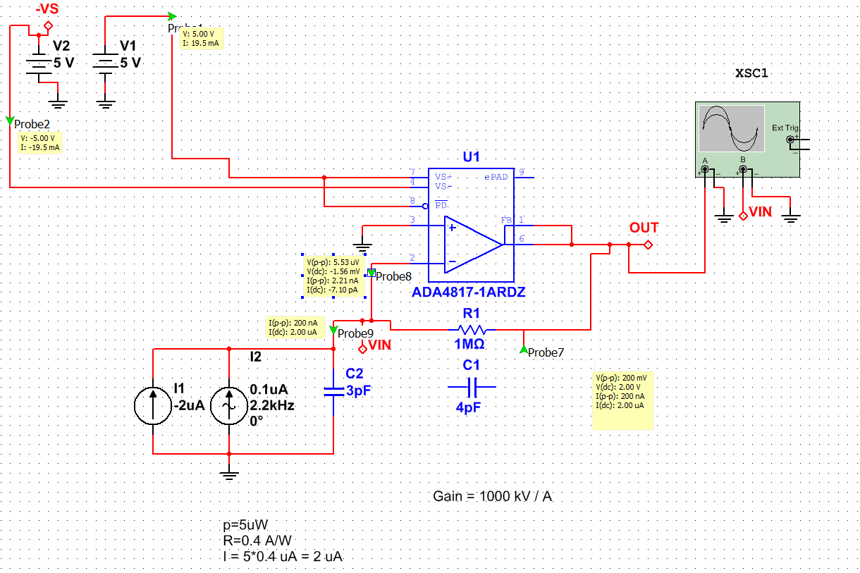
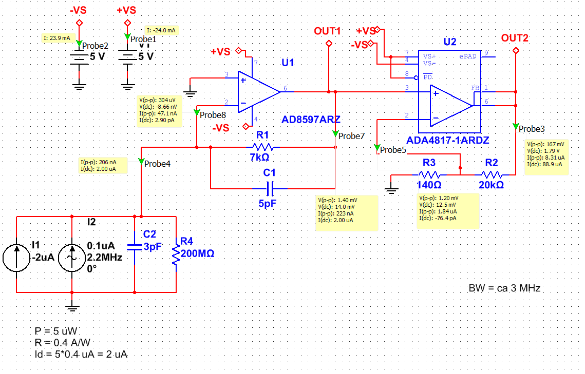
The first design is a single transimpedance-amplifier (TIA) using an ADA4817 and a 1 MOhm resistor. This isn't a great design, since the op-amp is much too fast compared to what is needed/required here. The second design is a 7 kOhm TIA (AD8597) followed by a ~140 V/V gain non-inverting amp (ADA4817). This gives the same total effective gain of ~1 MOhm.
These circuits were designed for a 2 V output with a 2 uA photocurrent produced by about 5 uW of HeNe laser light at 633 nm. The output will hit the "roof" (the positive rail) at about 12 uW of optical power.
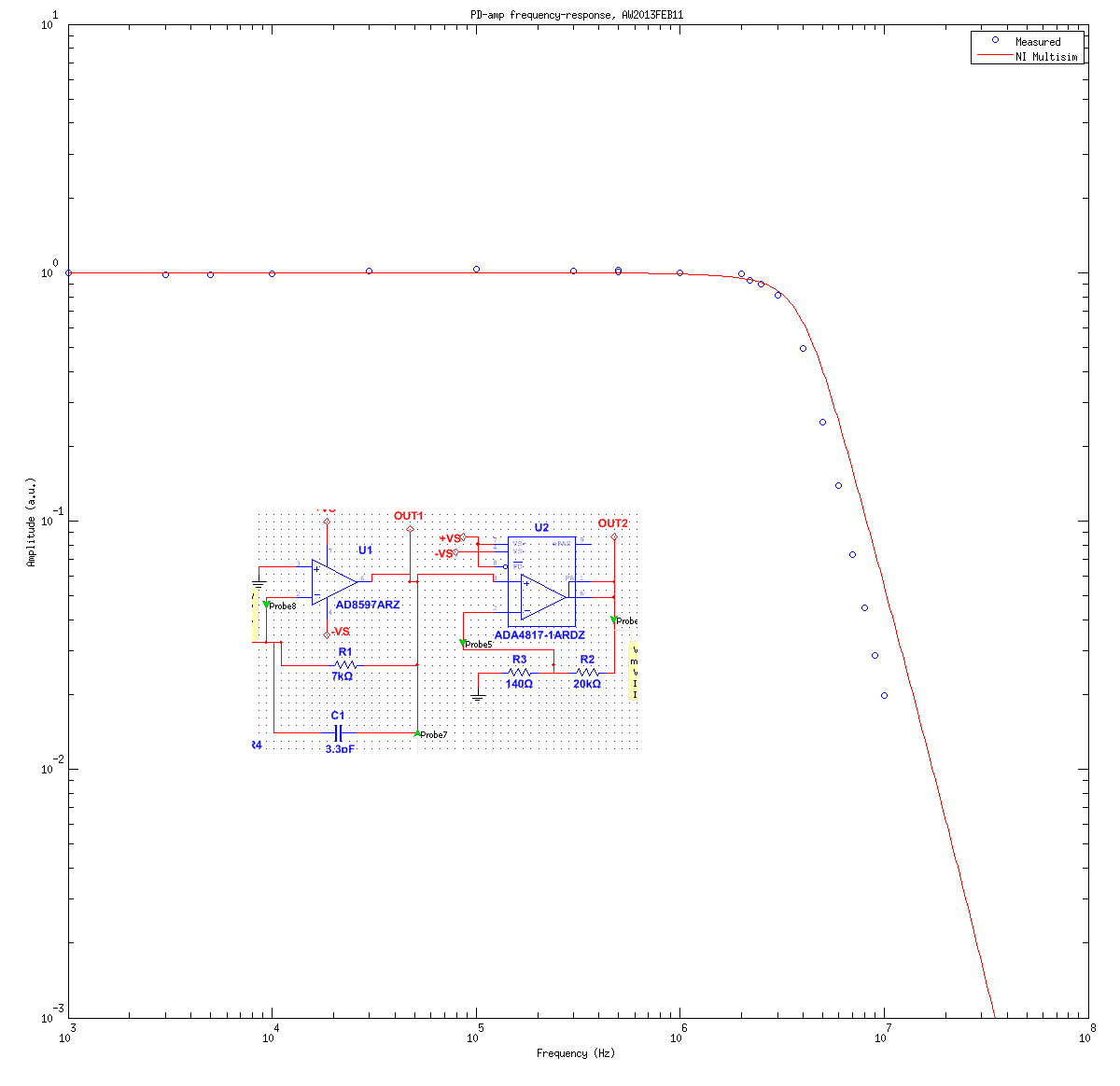
The agreement between simulation and experiment is not very good. I suspect my extremely simple LED-test is to blame. I should build a VCSEL circuit which allows testing these and other photodiode receivers to much higher frequencies.
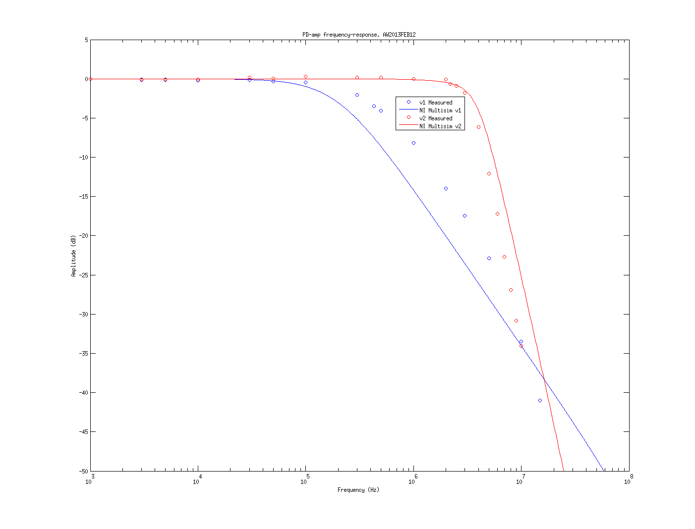
I assembled and tested the latest photodiode-amp today. I tested the frequency response using a red LED driven directly by an Agilent function-generator with an offset of 1.2 V and a 600 mVpp sine-wave. The LED datasheet doesn't specify a rise-time or bandwidth, but I'm hoping it is fast enough to test this 2-3 MHz receiver. I do have some small VCSELs that should be very fast and suitable for testing photodiode receivers up to 500 MHz and beyond.
The signal from the LED caused a 3 V output swing, which explains the slightly lower observed (large-signal) bandwidth compared to the simulated (small-signal) bandwidth. Some of the difference between the simulated frequency-response and the measured one is probably explained by stray capacitance which slightly lowers the bandwidth.
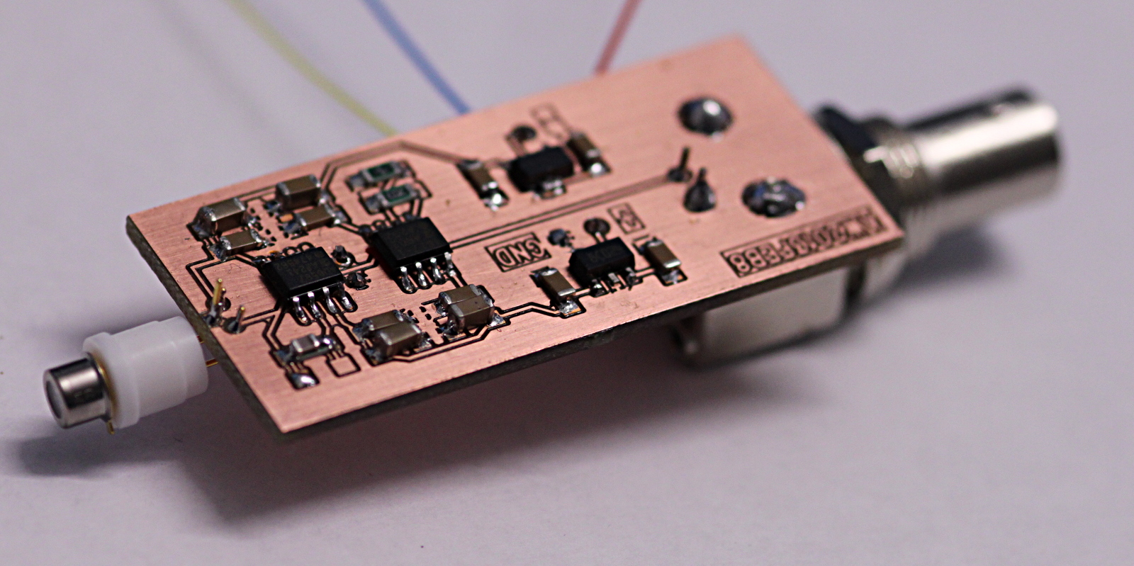
A revised version of the circuit and PCB for a photodiode amplifier, to be used in PDH-locking (Pound-Drever-Hall) as well as RAM-nulling (residual amplitude modulation) in a laser experiment I am doing. The changes compared to the first prototype are:
Here is a schematic and simulation results produced with the free version of NI Multisim from Analog Devices. The design is for roughly 1 MOhm of transimpedance gain in total, here split between 7 kV/A transimpedance gain, and 144 V/V for the non-inverting second op-amp. At 1 kV/A of transimpedance gain a 5 uW optical signal at 633 nm (HeNe laser!) that produces a 2 uA photocurrent will result in a 2 V output signal. The AC analysis shows very slight gain-peaking for the transimpedance-stage (red trace) and a -3 dB bandwidth of >3 MHz overall (green trace).
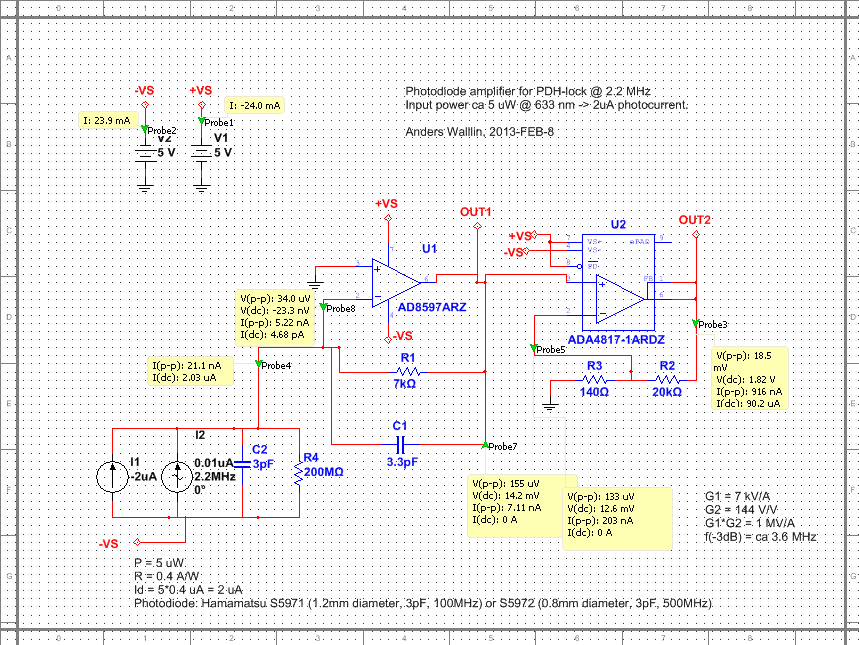
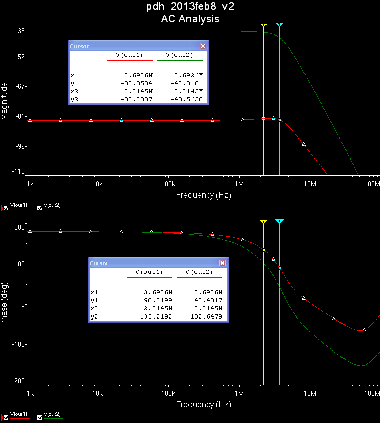
The first op-amp used in the transimpedance stage only needs to have a bandwidth slightly exceeding the transimpedance gain bandwidth (the feedback resistor R1 together with the compensating cap C1, the capacitance of the photodiode C2, and the input-capacitance (not shown) of the op-amp form an RC low-pass filter). The AD8597 is marketed as "ultralow distortion/noise" and is fast enough (10 MHz). The second non-inverting op-amp needs a high gain-bandwidth-product (GBP) since we are amplifying ~100-fold here. The ADA4817 has a small-signal bandwidth of 1 GHz and GBP~400 MHz, so should work OK here.
A voltage of only 14 mV over the transimpedance-resistor is not ideal. The Johnson noise (which in principle a good designer can control/minimize) in the resistor will dominate over the shot noise (which we cannot avoid) in the optical signal. For shot-noise limited performance the rule of thumb is to make the voltage drop at least 51 mV (which will make Johnson and shot noise equal). Without tricks however that is not possible as here we have both a weak signal (2 uA of photocurrent), we want a high gain (1 kV/A in total), and we want to go fast (~3 MHz bandwidth)! If you relax any of those requirements (more power, less gain, slower response) it is straightforward to build a shot-noise limited amplifier in one or two stages.
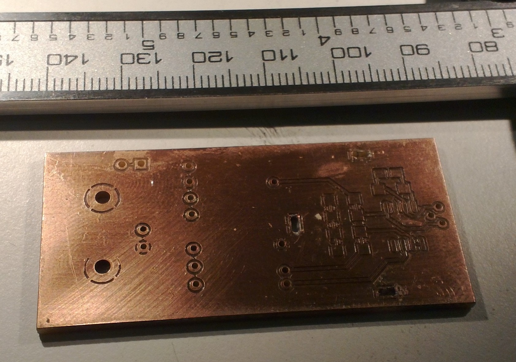
The PCB, fresh from the mill:
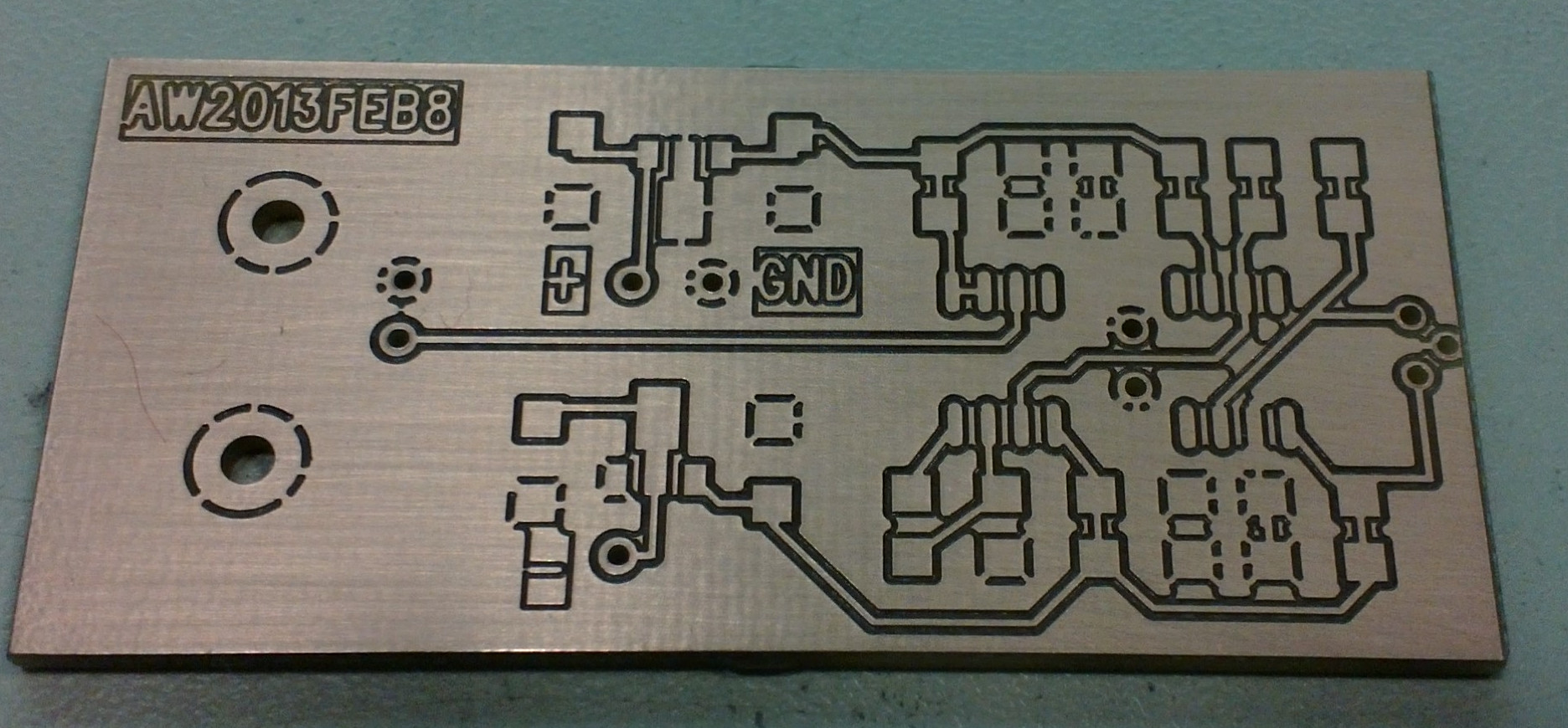
Far right is a 3-pin TO-18 socket for the photodiode. Right-middle are the two op-amps with their feedback-resistors/caps, as well as two de-coupling caps for both +5V and -5V. Left-middle are 7805 and 7905 voltage regulators, and the BNC output-connector is far left. All the surface mount components are mounted on the top layer of the board, while the through-hole components are bottom-mounted. Resistors and caps are 1206-size. This PCB should fit the earlier enclosures I turned on the lathe.
Hopefully I will have time to assemble and test one or two of these next week. I should measure the actual frequency-response and compare it with the simulated one.
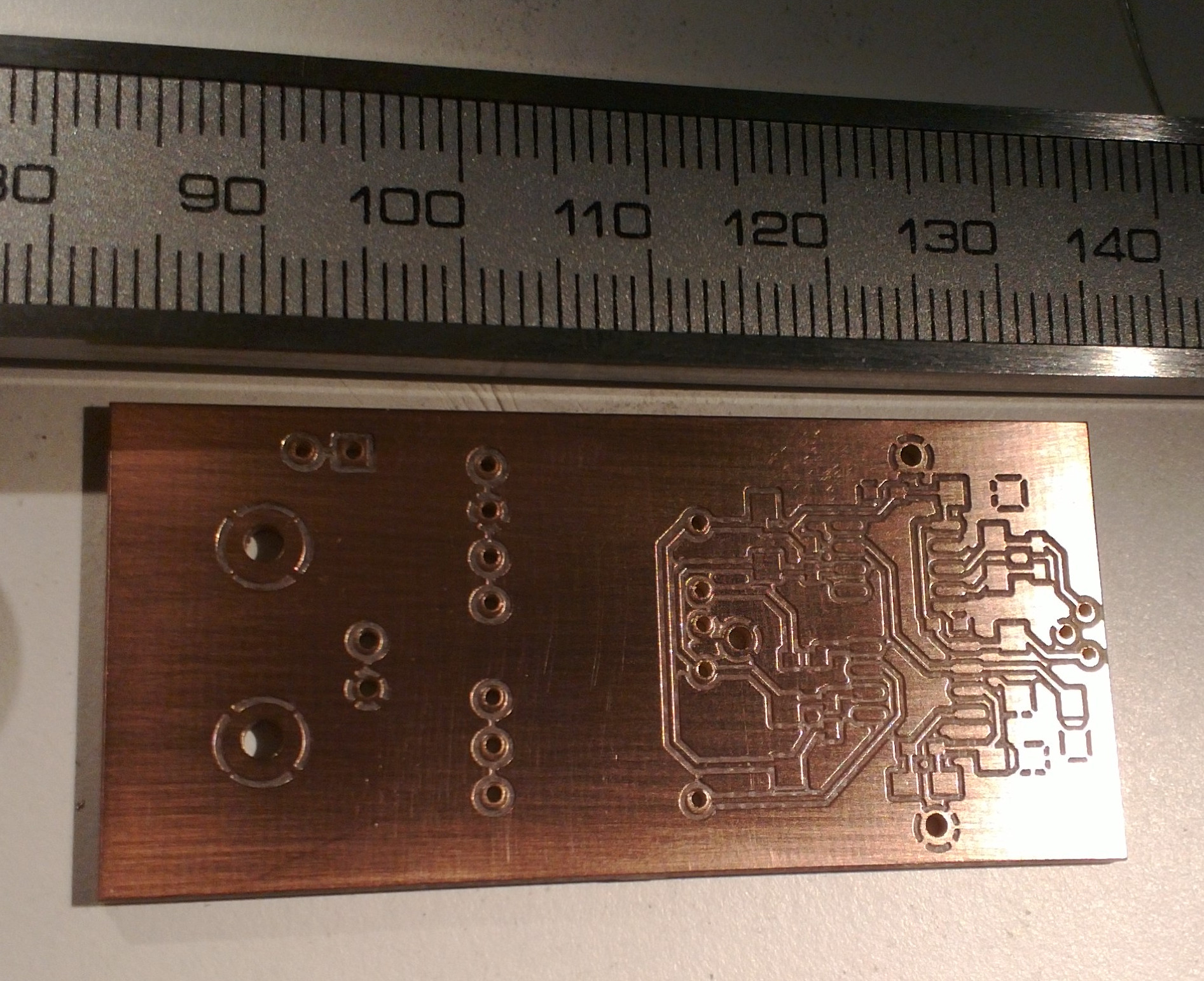
I made this PCB on the LPKF mill today:
Moments later, it was populated with components:
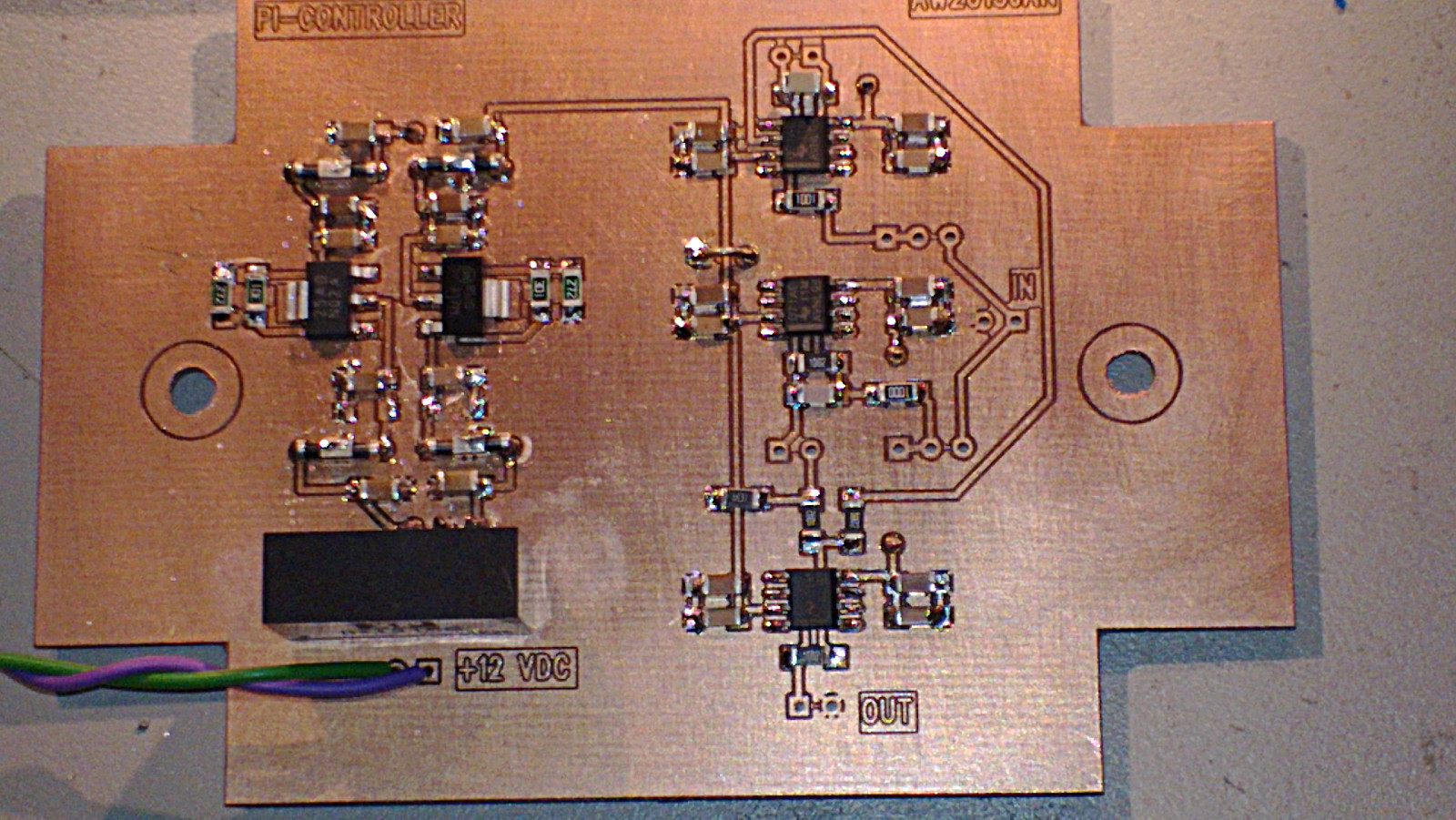
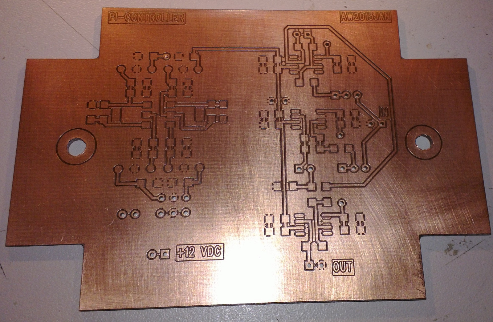
This is a PI-controller with three op-amps. One for the P-term, one for the I-term, and one that sums P+I.
The left side of the PCB is a +/-12V power-supply consisting of a DC2DC converter, caps and EMI-filters (Murata NFE61), LM337/LM317 adjustable voltage regulators, and more caps and EMI-filters. Despite the caps and filters I'm not sure this design gives good enough +/- 12V DC supplies for instrumentation use - when the DC2DC input comes from a typical cheap "wall-wart" switch-mode PSU. Or perhaps there is direct RF/capacitive cross-talk from the wall-wart input to the op-amp circuits which shows up as noise in the signal?
The PCB is shaped to fit a Fibox enclosure.
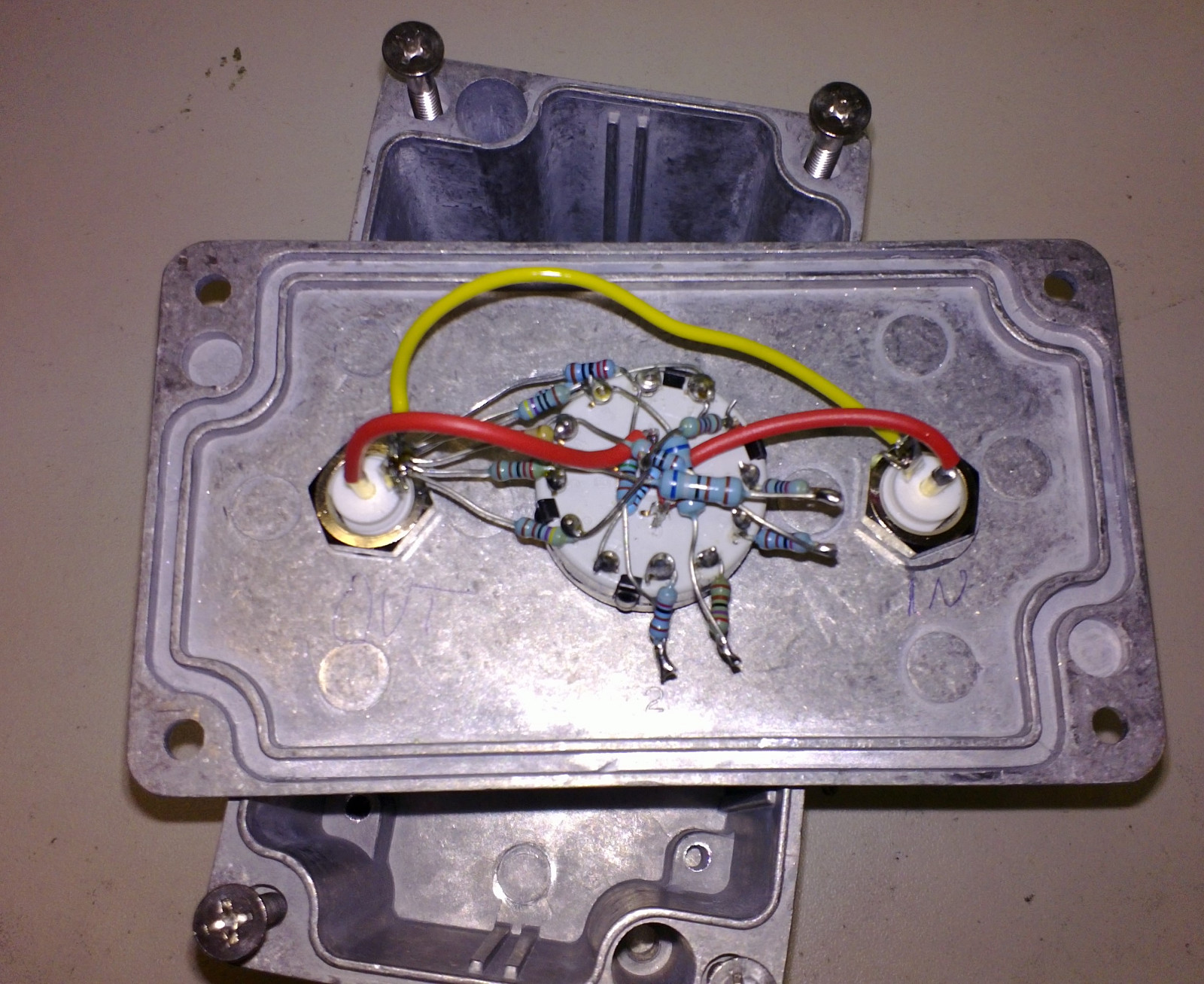
"Attenuator" is just a fancy word for voltage divider. This hack will not win many points for beauty:
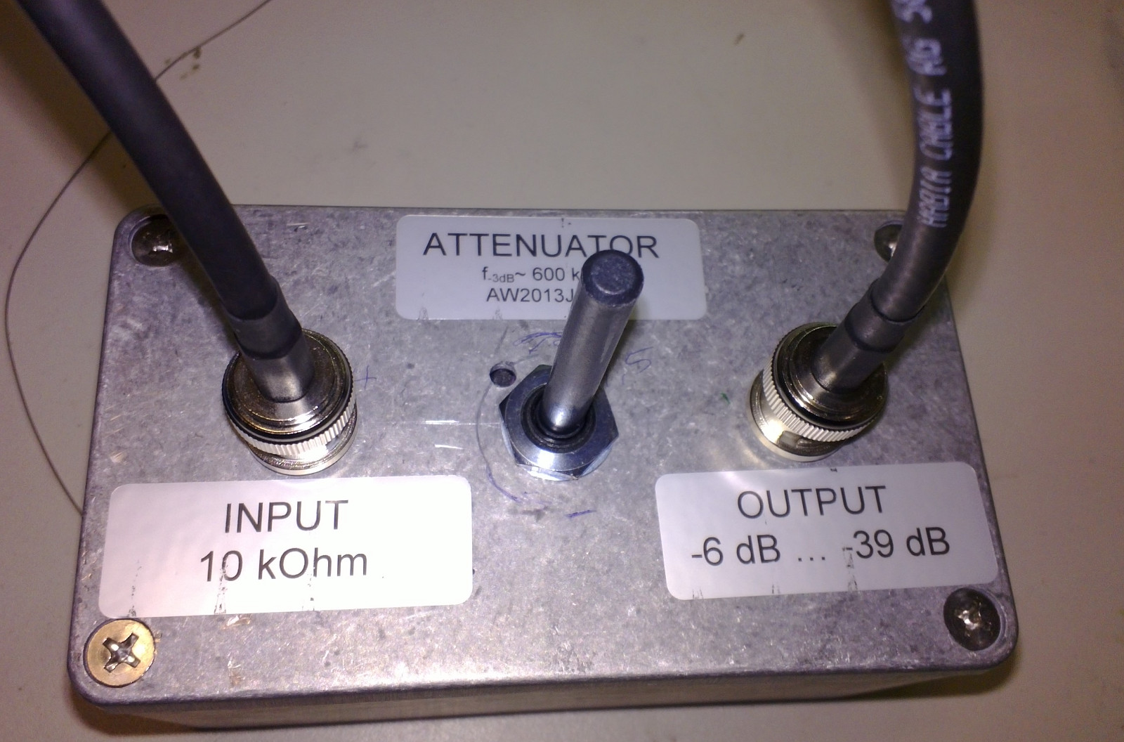
Enclosed in a box it looks nicer 🙂
This attenuator goes between two op-amp circuits where I figured the first circuit will be able to drive a 10 kOhm load, and the input impedance of the second circuit is high enough not to load the voltage divider too much.
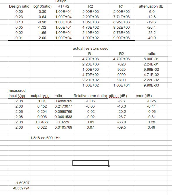
The back-of-the envelope design called for six voltage dividers with log-spaced attenuation between -6 dB and -40 dB. The input and output are connected to a 2-pole 6-position rotary switch that selects which voltage-divider is in use. The measured attenuation differs from the design by about 0.5 dB at most. For a large input-signal at the -6 dB attenuation setting the -3 dB bandwidth is about 600 kHz.
Design spreadsheet:
I've been measuring the beat-note (wikipedia talks about sound-waves, but it works for light-waves too) between two HeNe lasers. It jumps around maybe +/- 5 MHz quite rapidly which is not nice at all:
One laser is a commercial stabilized laser (I've tried both a HP5501A and a Mark-Tech 7900), and the other laser is a tunable one which I want to use for my experiment. But with this much jumping around the tunable laser is no good for the experiment I want to do 🙁
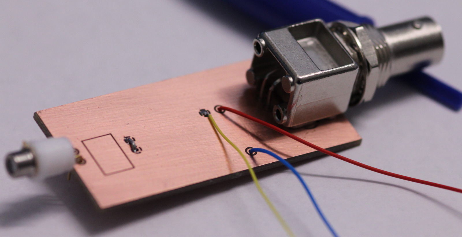
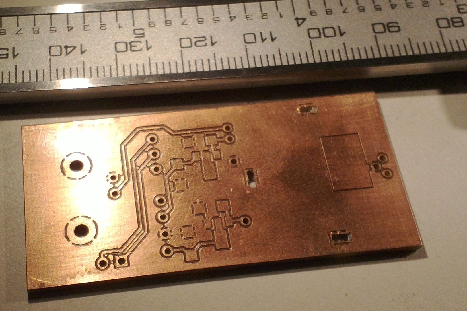
I made this PCB for a second photodiode amplifier today. This one is designed for higher light-levels and higher bandwidth. I will post the schematics along with measurement data when I've tested the circuit.
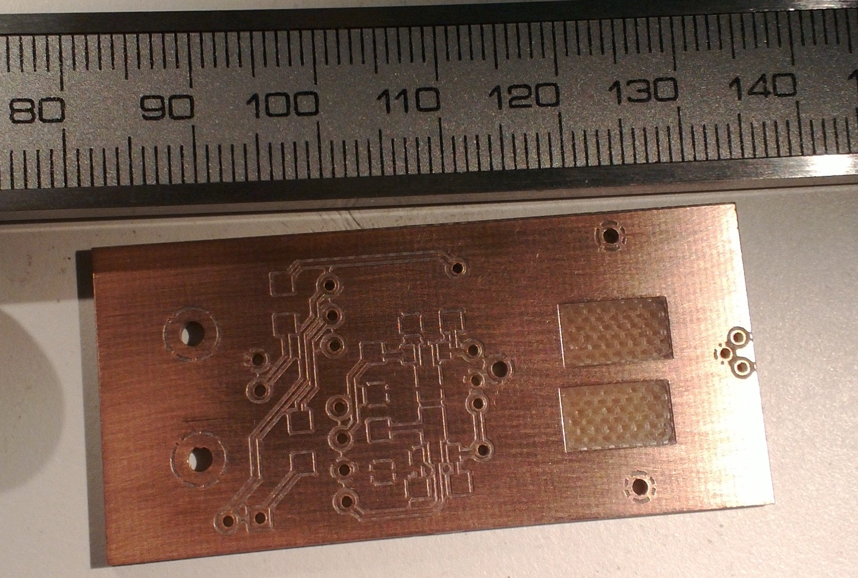
The V-cutter is designed to cut a slot that is nominally 8 mils (0.2 mm) wide, but the actual cut-width depends on how the z-axis is adjusted. Removing the ground-plane copper from under the high-speed op-amps is supposed to minimize stray capacitance.
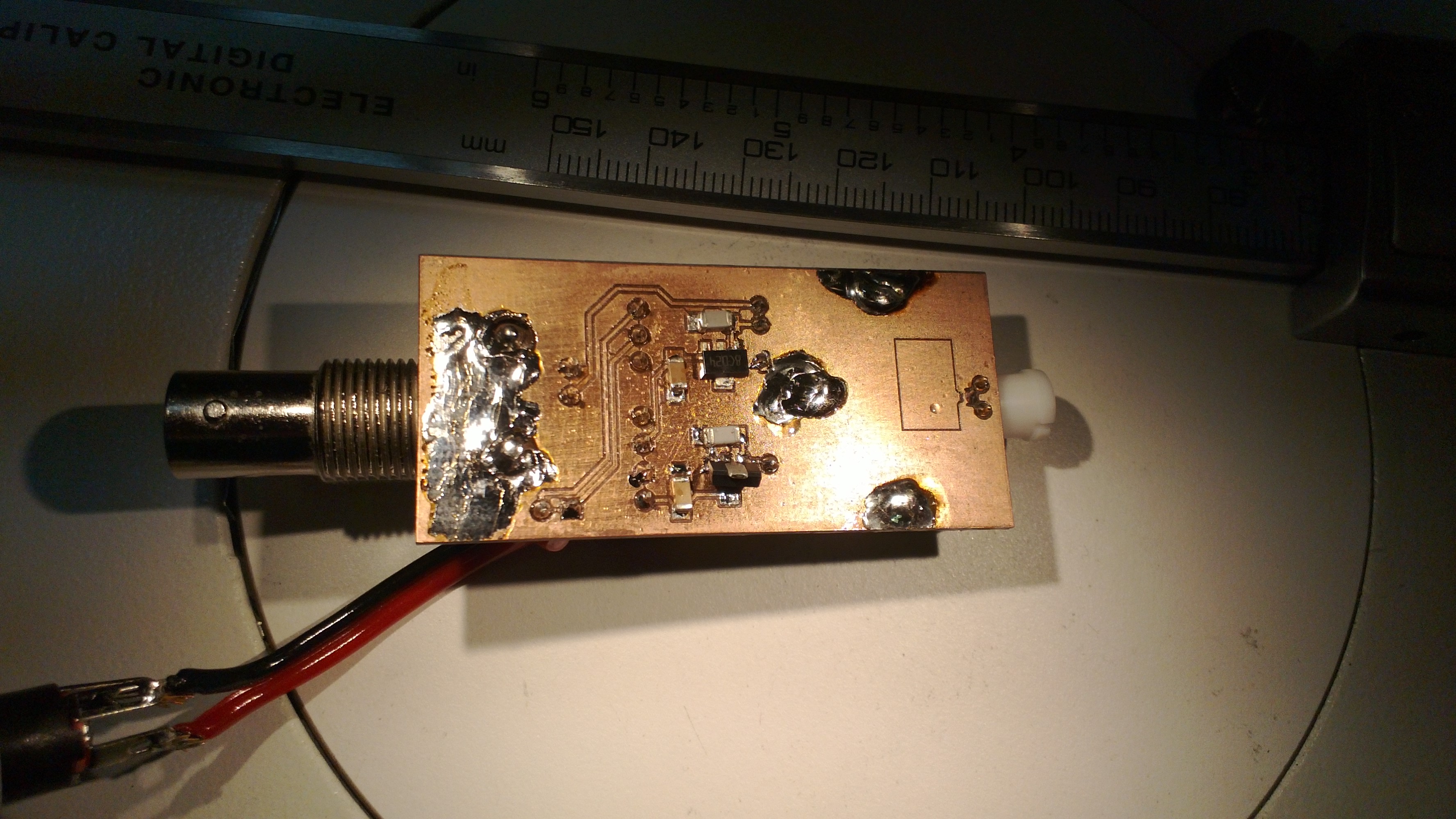
Some assembly of the PCB and enclosure for the first photodiode amplifier has happened today. Soldering the surface-mount components under a microscope was mostly easy - but trying to solder larger parts that require significant heating with the same tiny soldering iron used for small SMD parts was a mistake. The big parts were easy once I switched to a bigger soldering iron, but the BNC-connector was already a mess by then.
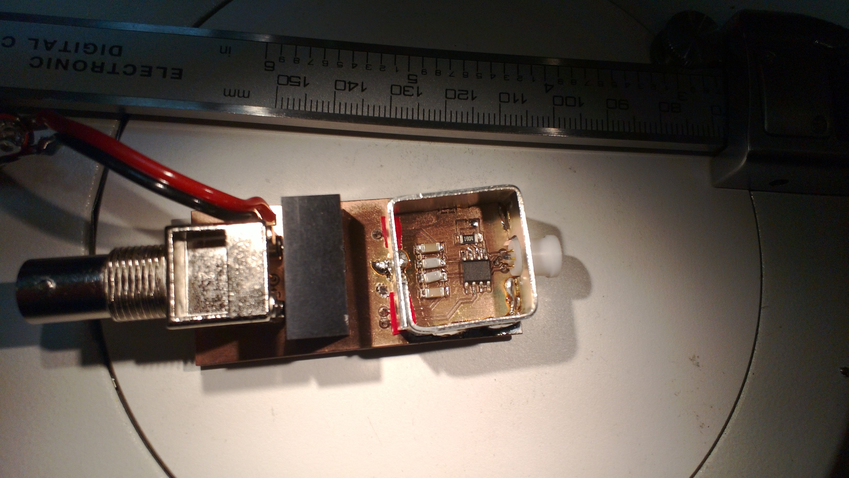
On the left a BNC connector. The black box in the middle is a DC-2-DC converter that produces +/-12VDC outputs from a single +9...18VDC input. The transimpedance amplifier on the right is based on an ADA4817 op-amp and is housed inside an RF screening can. On the far right is a white TO-18 socket for the photodiode.
The underside of the board has 7805 and 7905 voltage regulators that produce stable (hopefully!) +/-5V supply voltages for the op-amp.
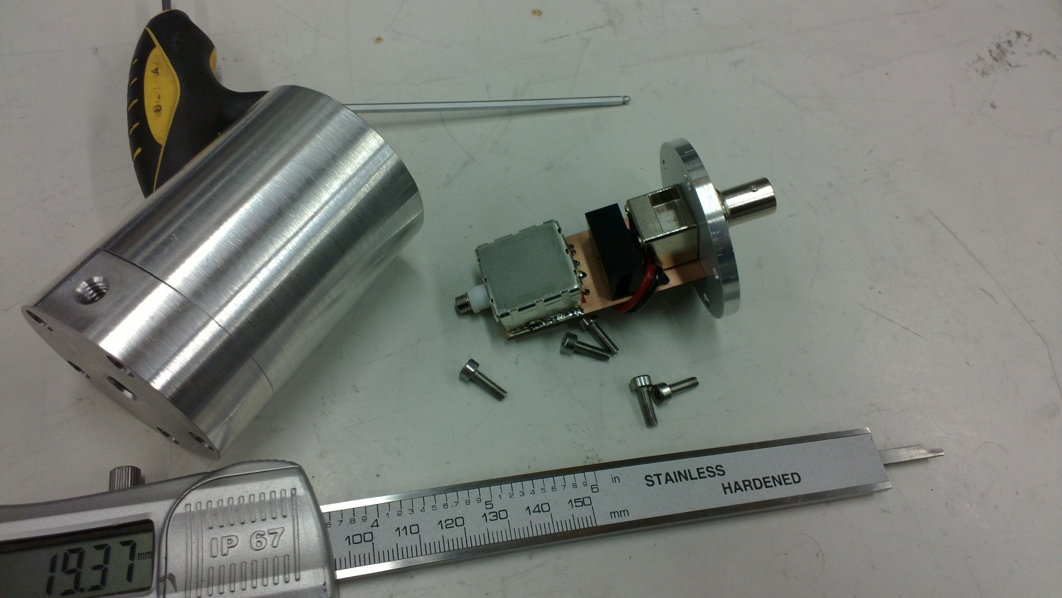
Here two holes have been drilled in to the back-plate for the BNC-commector (ca 12.2 mm diameter) and a DC-input jack (5.5mm diameter with a 2.5mm pin). The PCB is attached to the back-plate and slides into the body, while the photodiode looks out through the hole of the face-plate.
The only setback was a disagreement between the 1-2-3 pin-sequence in the datasheet vs. my PCB-software for the SOT-89 packaged 7905 negative voltage regulator. If you look closely you can see it is soldered up-side-down on this board because the PCB footprint is wrong.
I'm making photodiode (transmipedance) amplifiers, and here is the first PCB being milled today. In the foreground a test-run where the cutter-height was too low resulting in too thin or vanishing PCB-traces. Note how the PCB material is not held in place along the Z-axis at all. The PCB-blank is just located in X/Y on the table using two locating pins/holes. In the Z-direction the idea is that the pneumatic cylinder pushes the lower flange of the spindle into contact with the PCB-material, and the exact cutter-height is adjusted relative to this flange only.
The toolchain is (old!) commercial software: PADS PowerLogic for schematic design, PADS PowerPCB for PCB-design, CircuitCam for converting the gerbers to HPGL, which BoardMaster uses to drive the mill (over RS232).
For general purpose 3D CAD at work we have Vertex (a Finnish Inventor/SolidWorks clone) and I used it to draw a model of the amplifier:
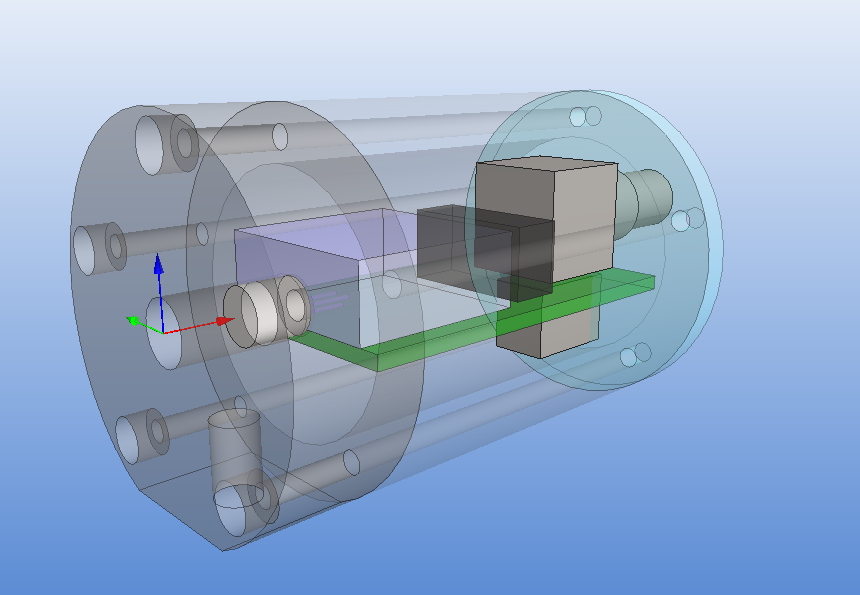
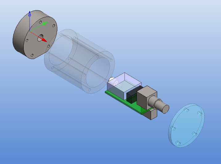
The size of the PCB and enclosure is mostly limited by how much of the powersupply one wants on-board, and how big connectors one wants to use. I'm using a standard BNC connector (SMA would have been smaller). The board is powered by a +9...18VDC supply which is DC2DC converted into +/-12 V and then regulated to +/- 5 V for the op-amp circuit. The box at the front is an RF shield for the amplifier itself. Light enters through an 8 mm hole in the face-plate and hits a TO-18 mounted photodiode. More on the circuit later.
The enclosure is 48 mm in diameter with a 16 mm thick face-plate, a 4 mm thick back-plate, and the body (55 mm length) bored out to an inner-diameter of 34 mm. The body should fit a 25x54mm PCB. The end-plates are attached to the body with five M3 screws on a 40 mm diameter bolt-circle. There is an M6 thread on the bottom of the face-plate, for attaching the amplifier to an optical-table or other instrumentation. I made two of these from 50 mm aluminium round-bar on a manual lathe and mill (using a rotary table for the holes/threads).
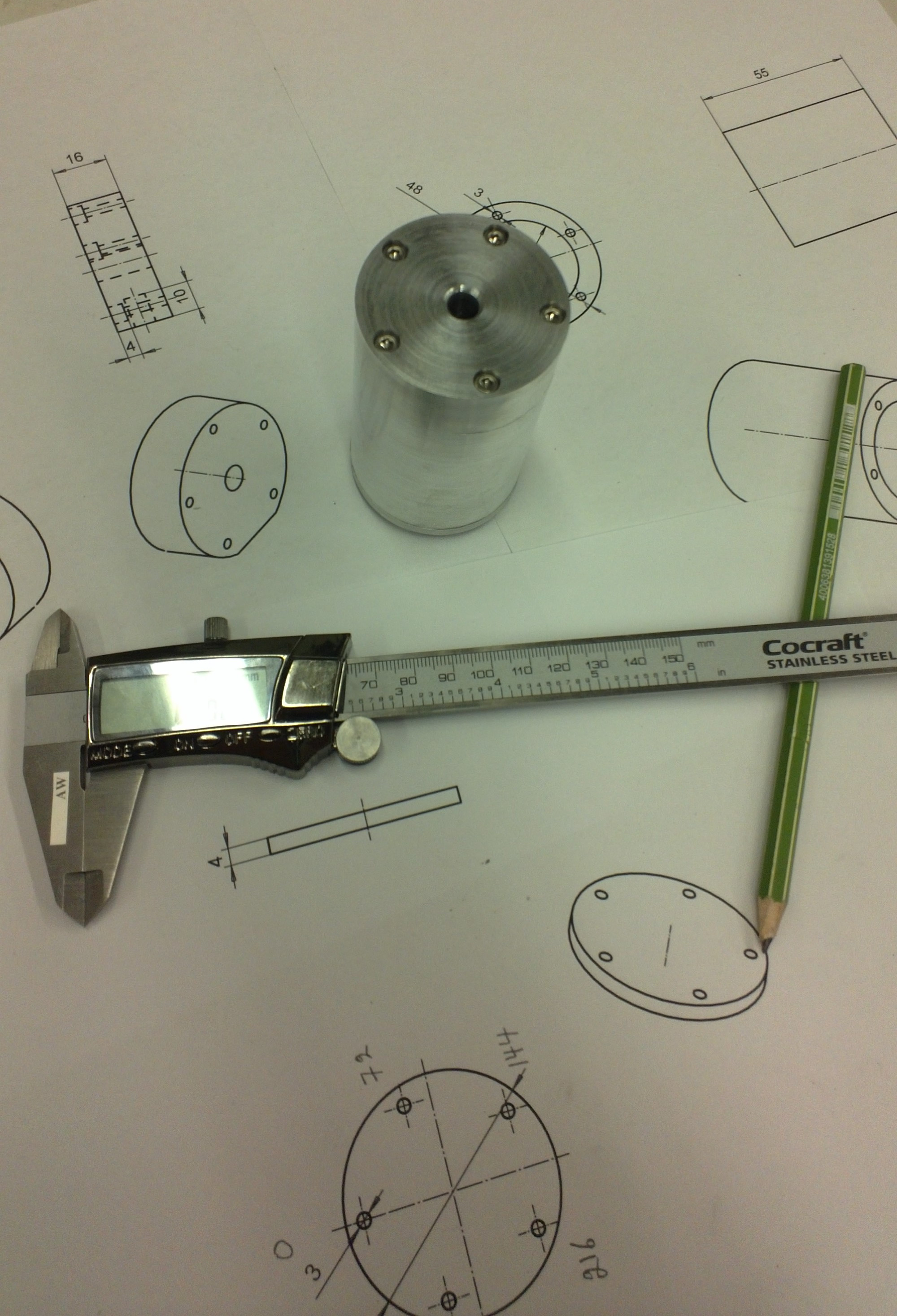
Note: for manual machining five evenly spaced holes the angle-sequence is: 0 - 72 - 144 - 216 - 288 - 0.
I'm thinking about polishing these a bit and then anodizing them. But for RF-shielding the contact-surfaces of all three parts would then have to be sanded/milled-down after andoizing. to ensure good electrical conductivity between the parts.