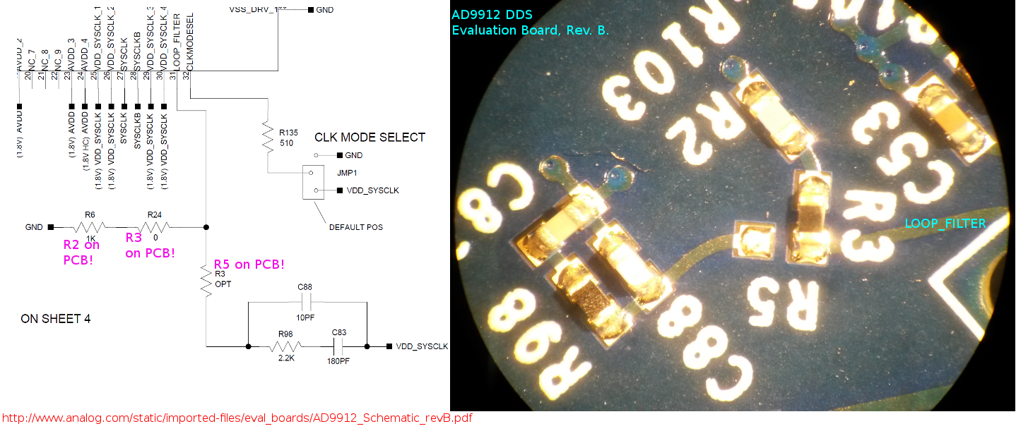
Update: it turns out the PLL filter components were not connected at all during the first tests I did 🙂 Here's a picture that compares the schematic against the actual board. When I changed the 0R resistor from position "R3" to position "R5" the PLL started behaving much more nicely. If anyone from AD is reading - please update your documentation!
With this change, and a 66x PLL multiplier giving a 10MHz x 66 = 660 MHz SYSCLOCK I get quite nice output:
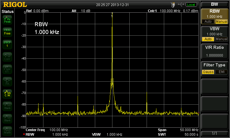
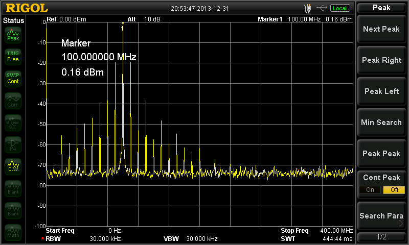
The output is set to 100 MHz and has an amplitude of ~0 dBm. There are -60 dBm spurs at +/- 50 kHz (not sure why?), -70 dBm spurs at +/- 10MHz, and a -65 dBm second harmonic at 200 MHz.
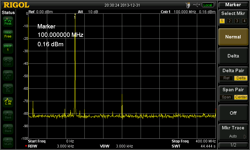
If I activate the "2x Reference" setting which detects both rising and falling edges of the input clock, and use that with a 40x PLL for a 10MHz x2 x40 = 800 MHz SYSCLOCK I still get very strong spurs at 10 MHz:
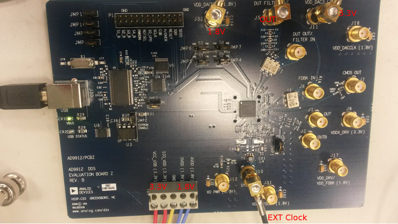
I have been testing this AD9912 DDS evaluation board:
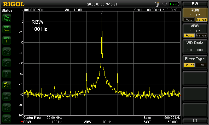
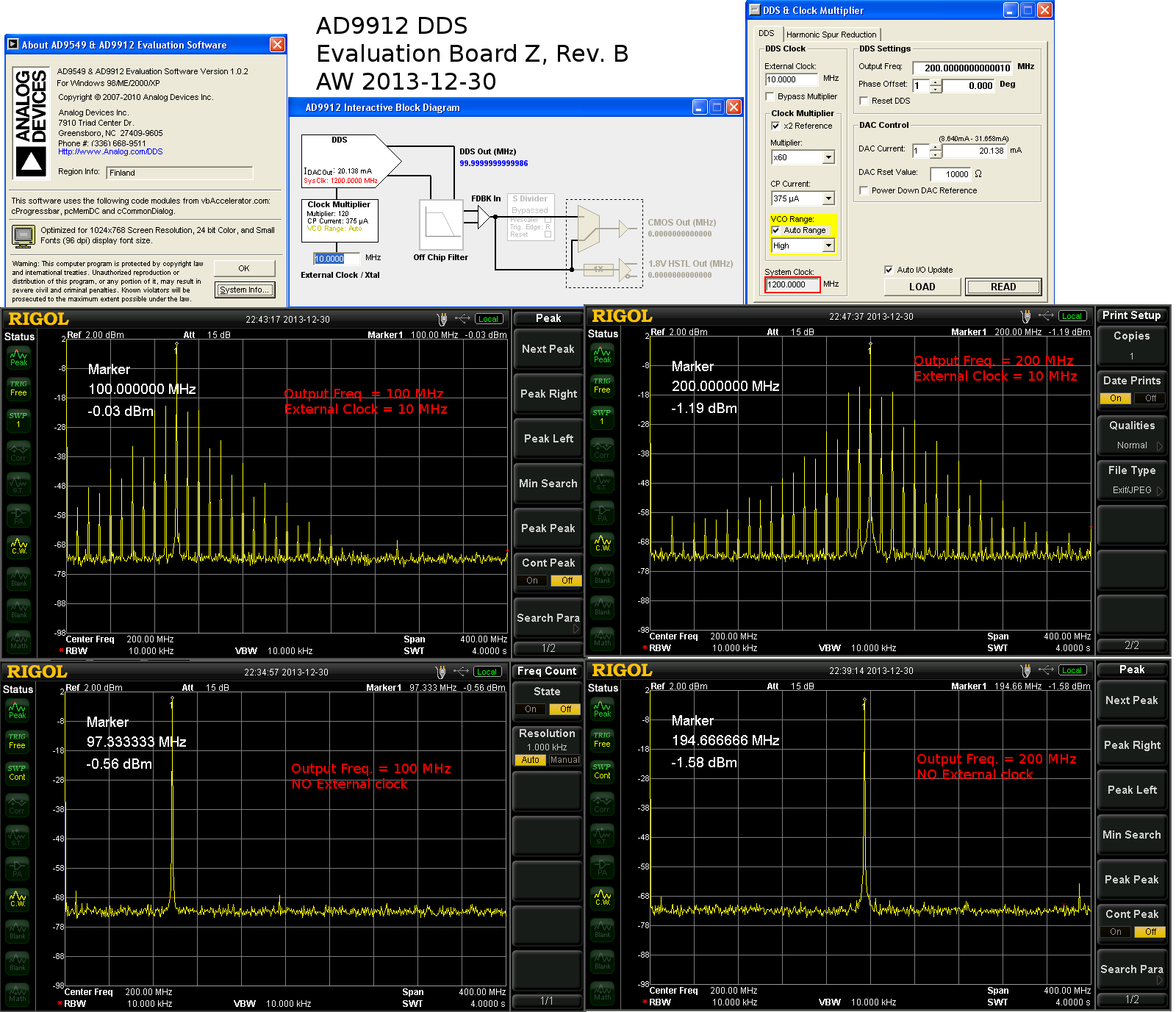
So far the results are a bit strange, with output as advertized only when no external input clock is supplied. Strange.
nice find on that loop filter. it is something unexpected