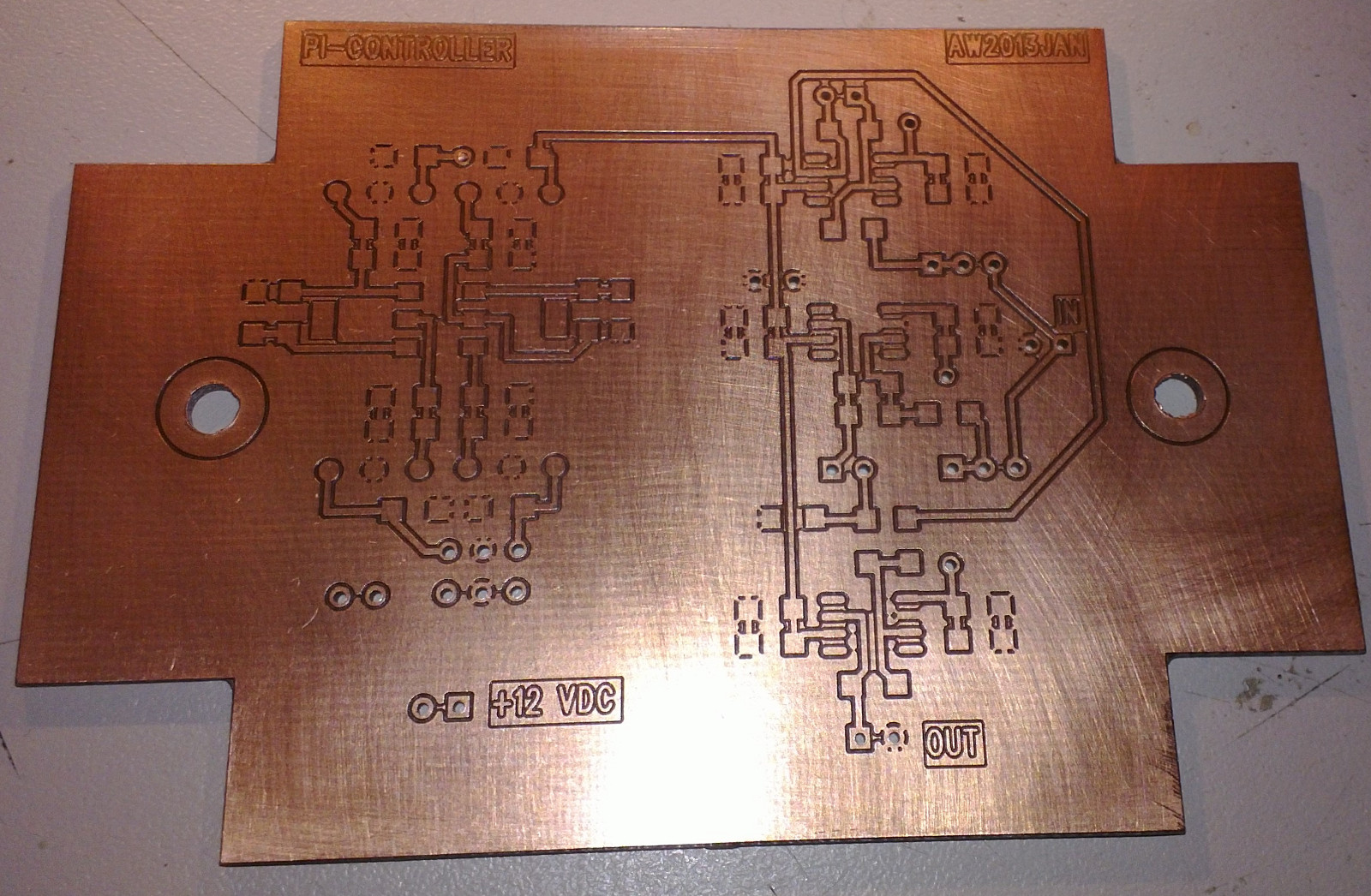
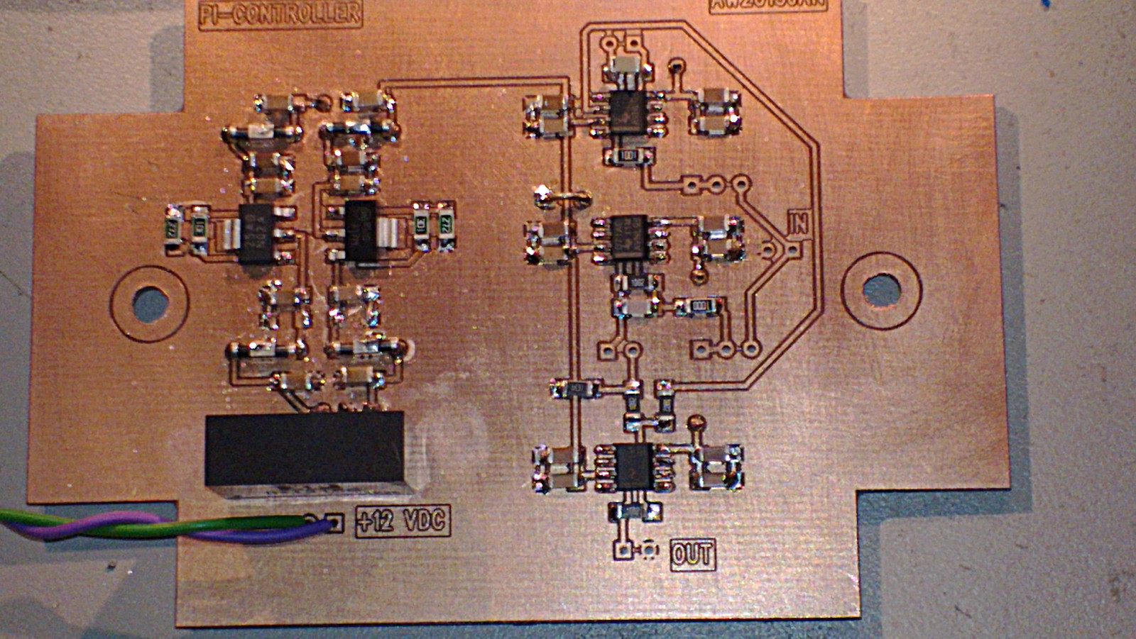
This is a PI-controller with three op-amps. One for the P-term, one for the I-term, and one that sums P+I.
The left side of the PCB is a +/-12V power-supply consisting of a DC2DC converter, caps and EMI-filters (Murata NFE61), LM337/LM317 adjustable voltage regulators, and more caps and EMI-filters. Despite the caps and filters I'm not sure this design gives good enough +/- 12V DC supplies for instrumentation use - when the DC2DC input comes from a typical cheap "wall-wart" switch-mode PSU. Or perhaps there is direct RF/capacitive cross-talk from the wall-wart input to the op-amp circuits which shows up as noise in the signal?
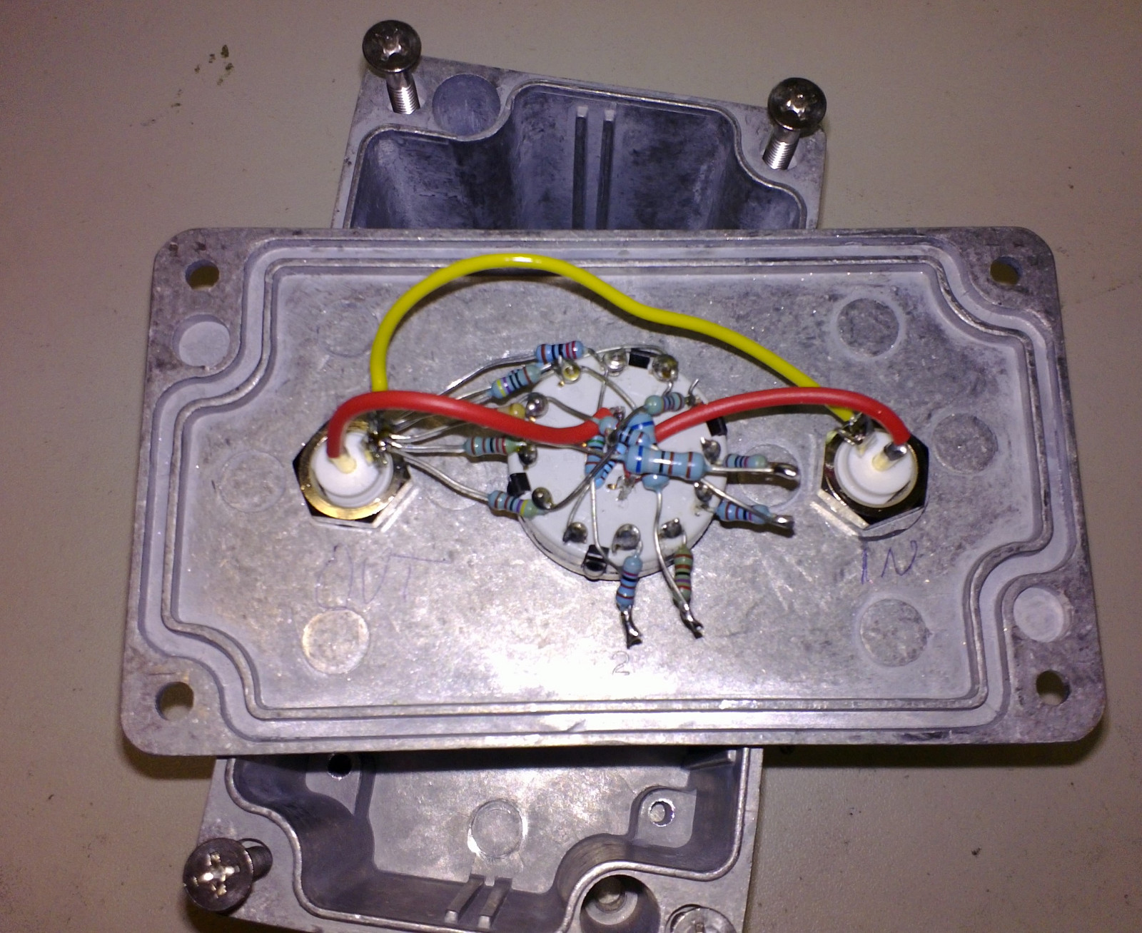
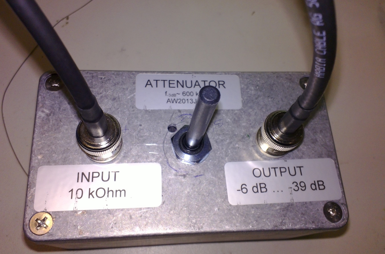
"Attenuator" is just a fancy word for voltage divider. This hack will not win many points for beauty:
Enclosed in a box it looks nicer 🙂
This attenuator goes between two op-amp circuits where I figured the first circuit will be able to drive a 10 kOhm load, and the input impedance of the second circuit is high enough not to load the voltage divider too much.
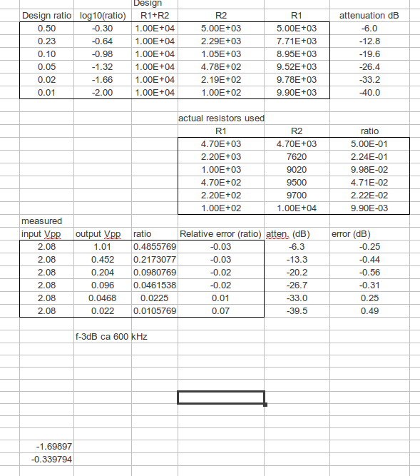
The back-of-the envelope design called for six voltage dividers with log-spaced attenuation between -6 dB and -40 dB. The input and output are connected to a 2-pole 6-position rotary switch that selects which voltage-divider is in use. The measured attenuation differs from the design by about 0.5 dB at most. For a large input-signal at the -6 dB attenuation setting the -3 dB bandwidth is about 600 kHz.
I've been measuring the beat-note (wikipedia talks about sound-waves, but it works for light-waves too) between two HeNe lasers. It jumps around maybe +/- 5 MHz quite rapidly which is not nice at all:
One laser is a commercial stabilized laser (I've tried both a HP5501A and a Mark-Tech 7900), and the other laser is a tunable one which I want to use for my experiment. But with this much jumping around the tunable laser is no good for the experiment I want to do 🙁
I made this PCB for a second photodiode amplifier today. This one is designed for higher light-levels and higher bandwidth. I will post the schematics along with measurement data when I've tested the circuit.
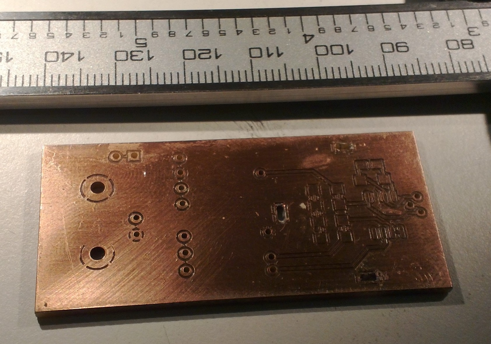
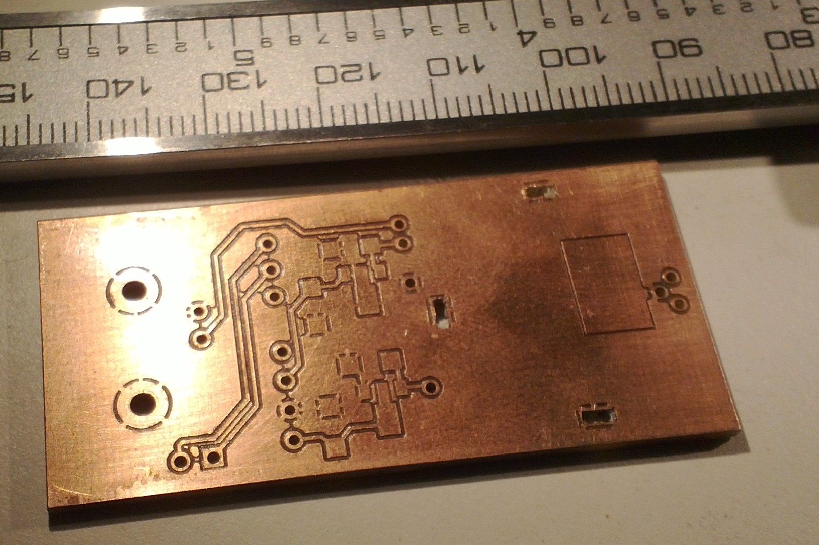
The V-cutter is designed to cut a slot that is nominally 8 mils (0.2 mm) wide, but the actual cut-width depends on how the z-axis is adjusted. Removing the ground-plane copper from under the high-speed op-amps is supposed to minimize stray capacitance.
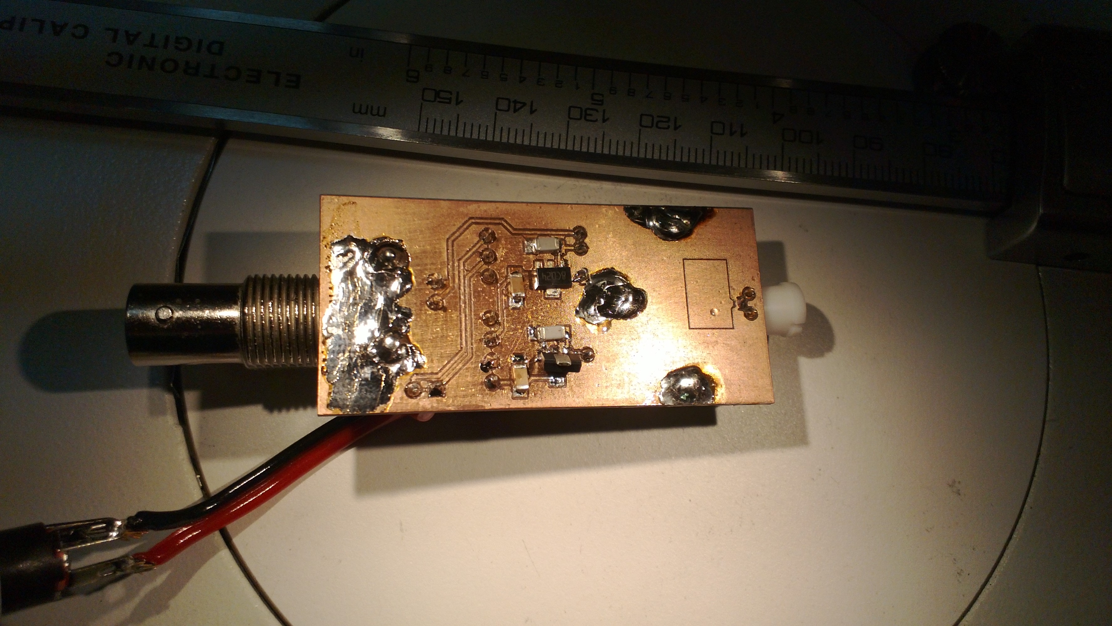
Some assembly of the PCB and enclosure for the first photodiode amplifier has happened today. Soldering the surface-mount components under a microscope was mostly easy - but trying to solder larger parts that require significant heating with the same tiny soldering iron used for small SMD parts was a mistake. The big parts were easy once I switched to a bigger soldering iron, but the BNC-connector was already a mess by then.
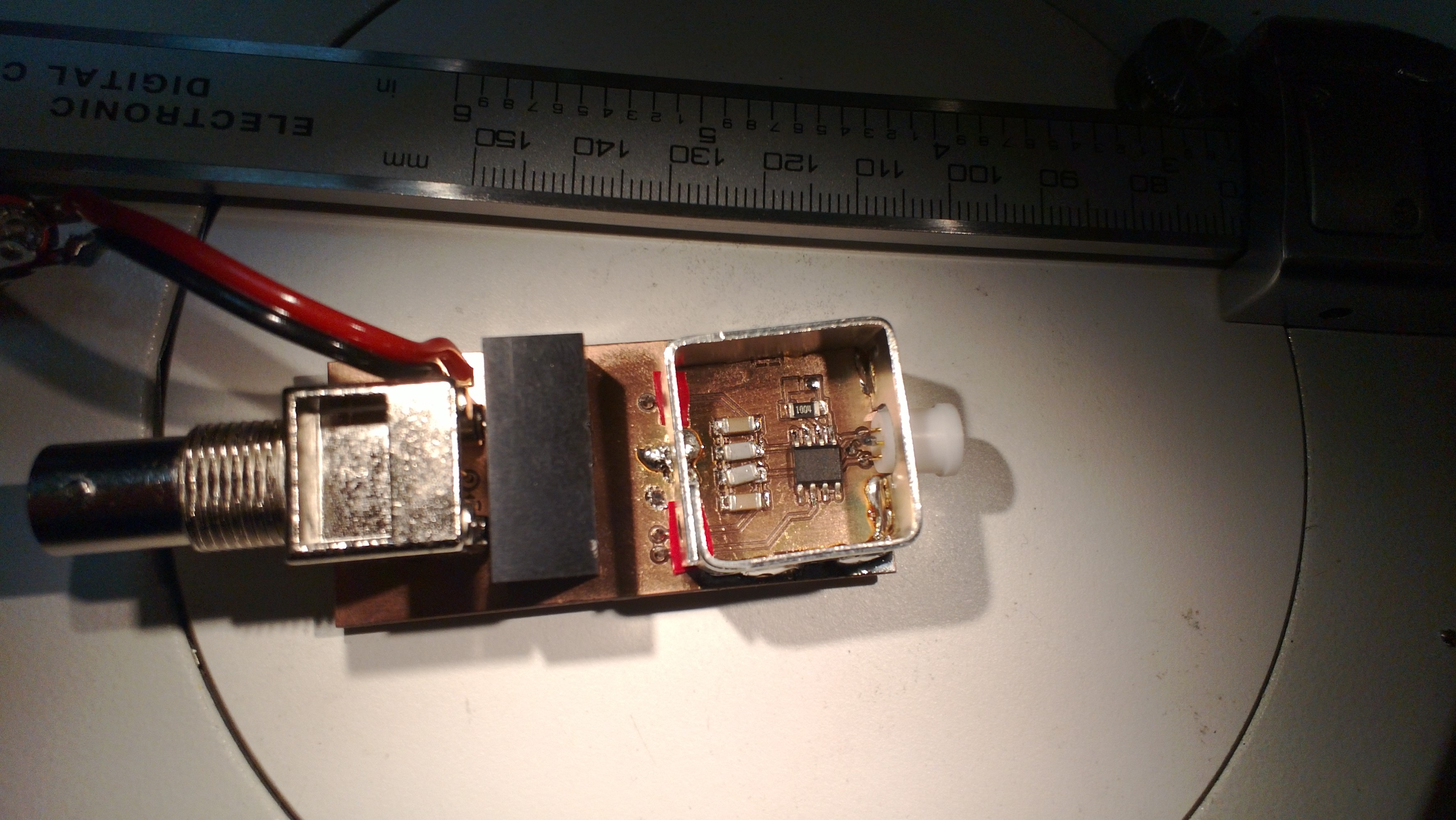
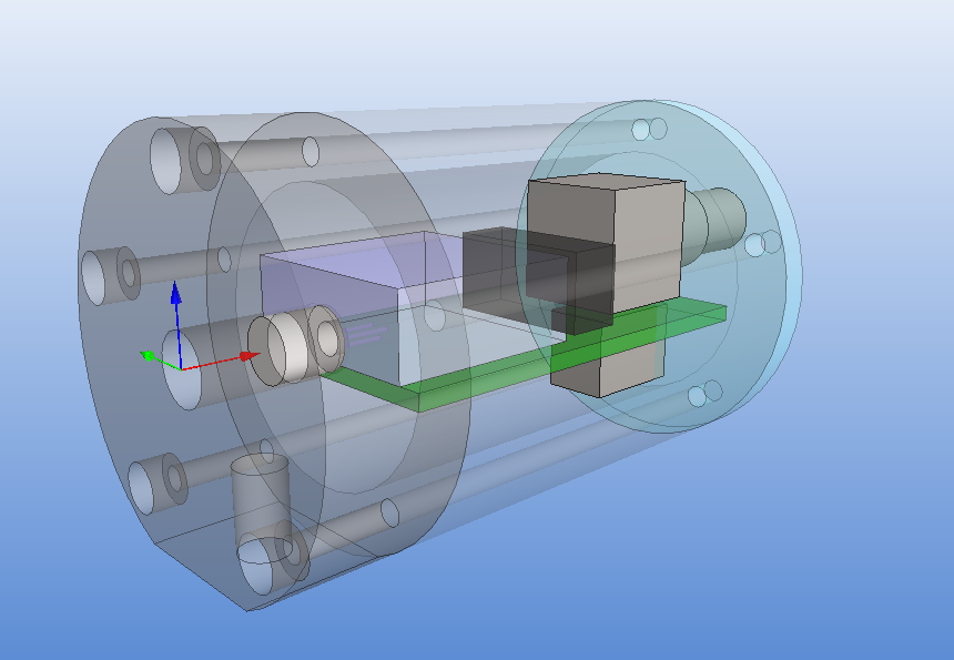
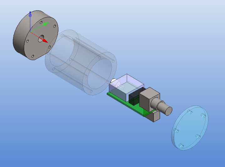
On the left a BNC connector. The black box in the middle is a DC-2-DC converter that produces +/-12VDC outputs from a single +9...18VDC input. The transimpedance amplifier on the right is based on an ADA4817 op-amp and is housed inside an RF screening can. On the far right is a white TO-18 socket for the photodiode.
The underside of the board has 7805 and 7905 voltage regulators that produce stable (hopefully!) +/-5V supply voltages for the op-amp.
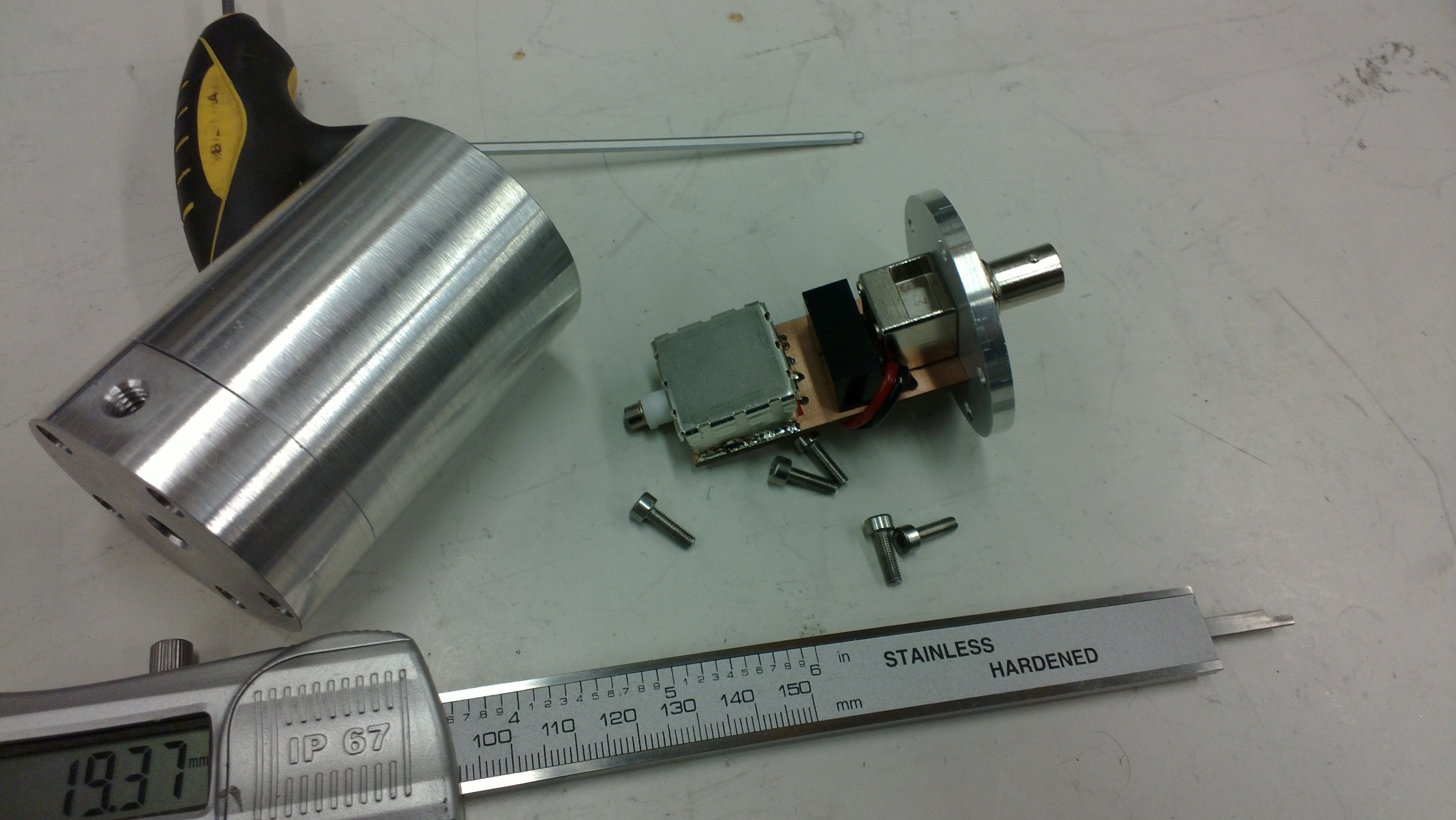
Here two holes have been drilled in to the back-plate for the BNC-commector (ca 12.2 mm diameter) and a DC-input jack (5.5mm diameter with a 2.5mm pin). The PCB is attached to the back-plate and slides into the body, while the photodiode looks out through the hole of the face-plate.
The only setback was a disagreement between the 1-2-3 pin-sequence in the datasheet vs. my PCB-software for the SOT-89 packaged 7905 negative voltage regulator. If you look closely you can see it is soldered up-side-down on this board because the PCB footprint is wrong.
I'm making photodiode (transmipedance) amplifiers, and here is the first PCB being milled today. In the foreground a test-run where the cutter-height was too low resulting in too thin or vanishing PCB-traces. Note how the PCB material is not held in place along the Z-axis at all. The PCB-blank is just located in X/Y on the table using two locating pins/holes. In the Z-direction the idea is that the pneumatic cylinder pushes the lower flange of the spindle into contact with the PCB-material, and the exact cutter-height is adjusted relative to this flange only.
The toolchain is (old!) commercial software: PADS PowerLogic for schematic design, PADS PowerPCB for PCB-design, CircuitCam for converting the gerbers to HPGL, which BoardMaster uses to drive the mill (over RS232).
For general purpose 3D CAD at work we have Vertex (a Finnish Inventor/SolidWorks clone) and I used it to draw a model of the amplifier:
The size of the PCB and enclosure is mostly limited by how much of the powersupply one wants on-board, and how big connectors one wants to use. I'm using a standard BNC connector (SMA would have been smaller). The board is powered by a +9...18VDC supply which is DC2DC converted into +/-12 V and then regulated to +/- 5 V for the op-amp circuit. The box at the front is an RF shield for the amplifier itself. Light enters through an 8 mm hole in the face-plate and hits a TO-18 mounted photodiode. More on the circuit later.
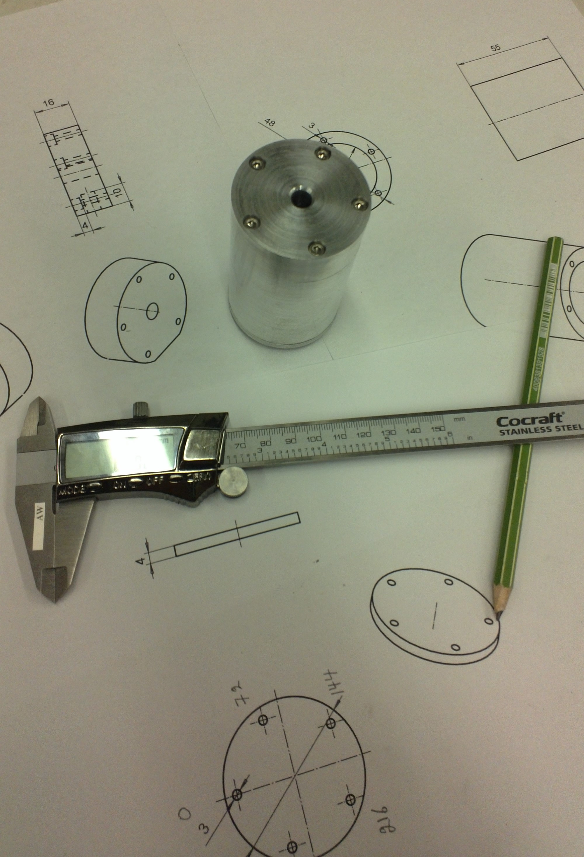
The enclosure is 48 mm in diameter with a 16 mm thick face-plate, a 4 mm thick back-plate, and the body (55 mm length) bored out to an inner-diameter of 34 mm. The body should fit a 25x54mm PCB. The end-plates are attached to the body with five M3 screws on a 40 mm diameter bolt-circle. There is an M6 thread on the bottom of the face-plate, for attaching the amplifier to an optical-table or other instrumentation. I made two of these from 50 mm aluminium round-bar on a manual lathe and mill (using a rotary table for the holes/threads).
Note: for manual machining five evenly spaced holes the angle-sequence is: 0 - 72 - 144 - 216 - 288 - 0.
I'm thinking about polishing these a bit and then anodizing them. But for RF-shielding the contact-surfaces of all three parts would then have to be sanded/milled-down after andoizing. to ensure good electrical conductivity between the parts.