OPA188, zero-drift op-amp in SOT-23 and SOIC-8. Input offset voltage drift ±0.03 uV/C typically.
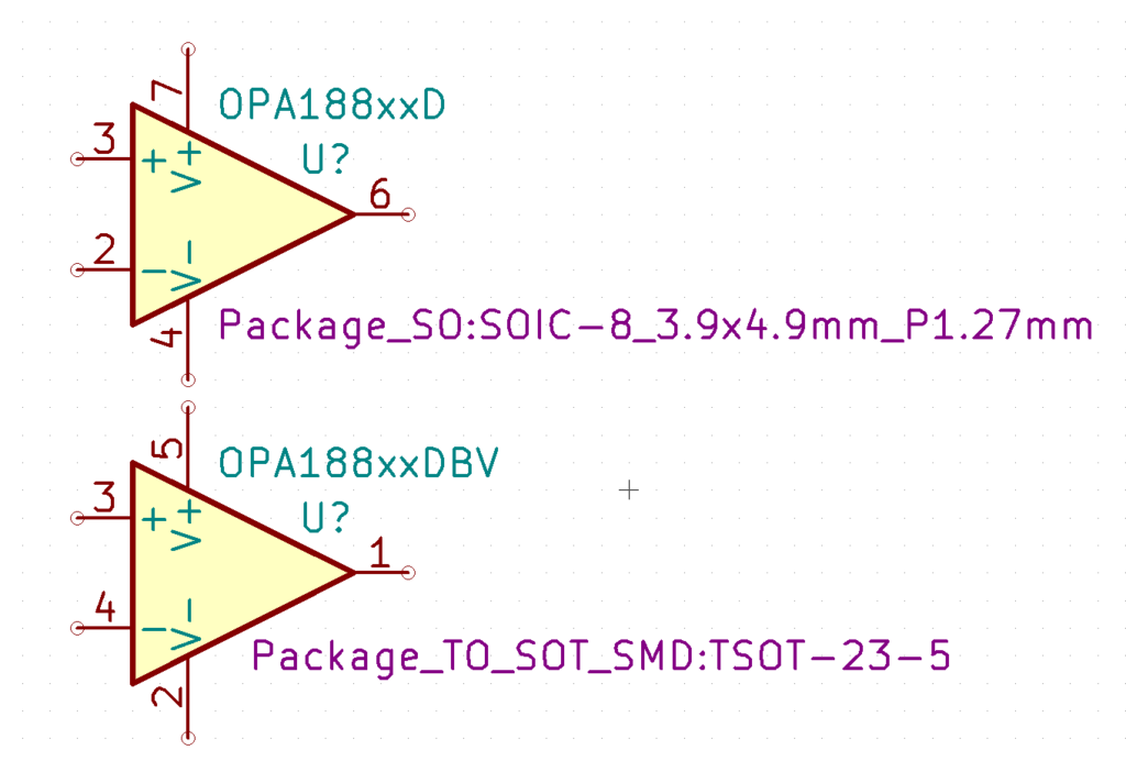
OPA188, zero-drift op-amp in SOT-23 and SOIC-8. Input offset voltage drift ±0.03 uV/C typically.
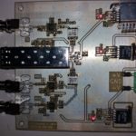
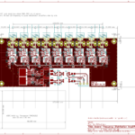
This is the fourth version of an interface board to Small Form Factor Pluggable optical transcievers (SFPs) with a bandwidth of >500 MHz. These are useful for various time/frequency experiments, with a measured frequency stability of <1e-13 @ 1s (in 0.5 or 5 Hz bandwidth) - perhaps slightly depending on what SFP is used. The SFP allows sending the signal along a single-mode fiber for 1-100 km easily.
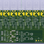
ADT2-1T converts to and from differential signals while LMH6702 op-amps provide 3 dB gain. There are parallel outputs on the RX pins. The current-draw on +3V3 by the SFP is quite high - usually requiring heat-sinking on the voltage-regulator
KiCad files available on request.
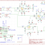
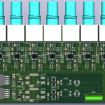
1:8 frequency distribution amplifier based on LMH6702 and LMH6609 op-amps.
In particular the power-supply section using a common-mode choke, a Murata BNX025 filter, and low-noise regulators LT1963 and LT3015 seems to work quite well. I also used ferrites (2 kOhm @ 100 MHz) as well as an RC-filter on all supply pins. Perhaps overkill? Performance with the intended AC/DC brick is still to be verified.
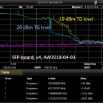
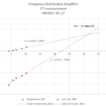
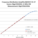
Measurements around 10 MHz show a 1 dB compression at over 14 dBm and an IP3 of around 27 to 30 dBm. The gain extends beyond 100 MHz with some gain-peaking.
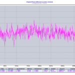
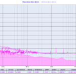
Some measurements of residual phase-noise with a 3120A phase-meter, at 10 MHz. My earlier distribution amplifier required shielding with aluminium foil as well as powering from a lead-acid battery to achieve a reasonably quiet phase-noise spectrum. These measurements were done with lab power-supplies for +/-12 V to the board and without any shielding.
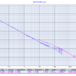
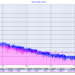
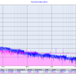
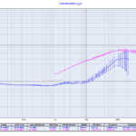
Finally some measurements of gain vs. frequency with a Rigol spectrum analyzer.
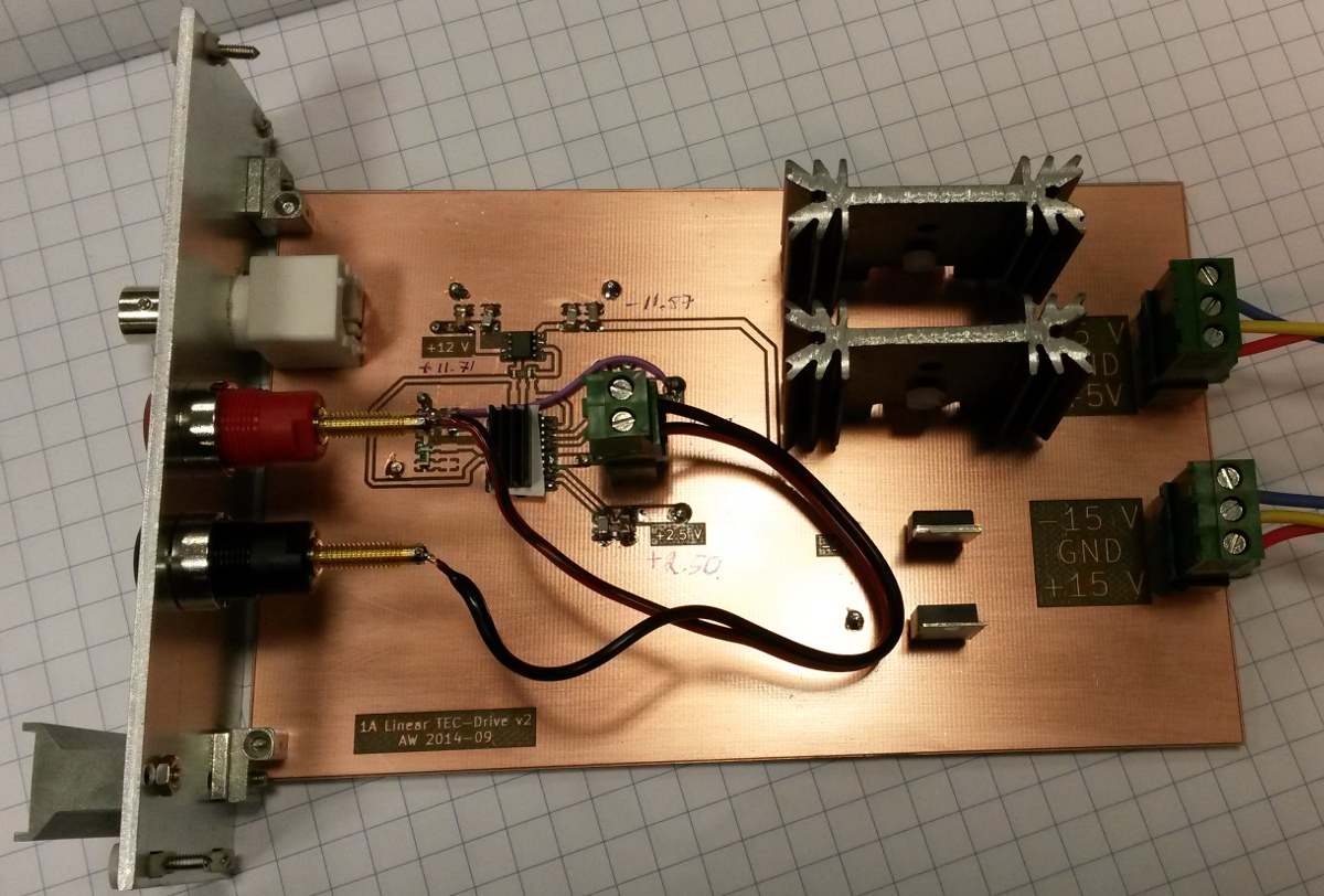
Sadly TEC-Drive v1 died an untimely death when it overheated due to being powered from +/-15 V instead of the designed +/-5 V.
TEC-Drive v2 is a simplified design using TO-220 packaged LM317/LM337 adjustable regulators and the OPA569 high-current op-amp.
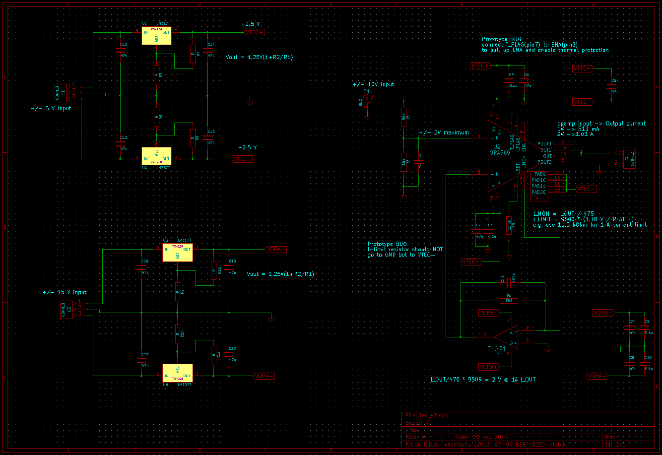
Constant-current drive is achieved using the OPA569 (U2) I_monitor output. I_monitor sources/sinks a fraction I_out/475 of the actual output current. By using another op-amp (U1) in a transimpedance configuration we get a feedback-voltage proportional to the output current.
PCB layout on a 100 mm x 160 mm eurocard:
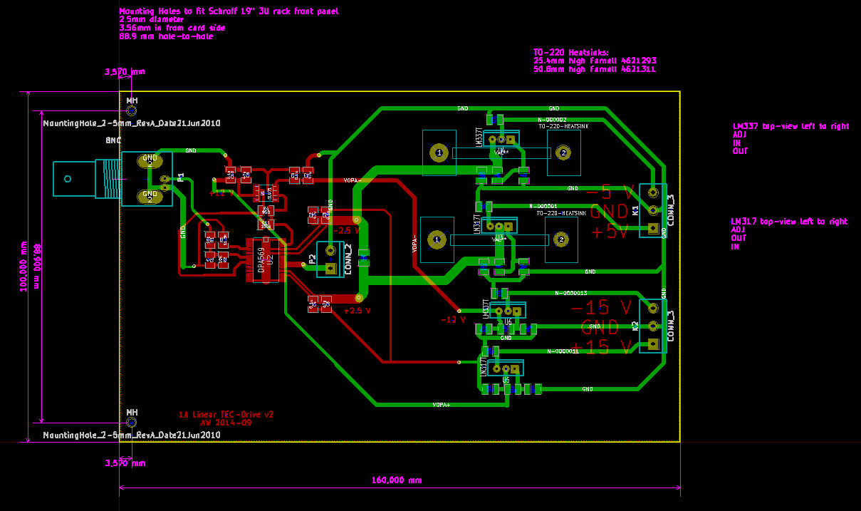
Built and assembled as a plug-in card for a 3U rack. Note big heatsinks on the +/-2.5 V regulators.
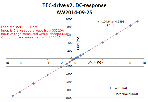
The DC-response is I_out = 105 mA/V * V_in, with an offset at zero-input of -4 mA.
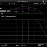
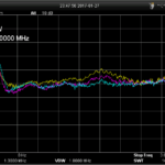
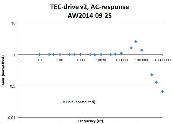
With no low-pass capacitors (C1 at the input, and C11 over the transimpedance-resistor) added and a purely resistive load the frequency response extends beyond 1 MHz with some ringing.
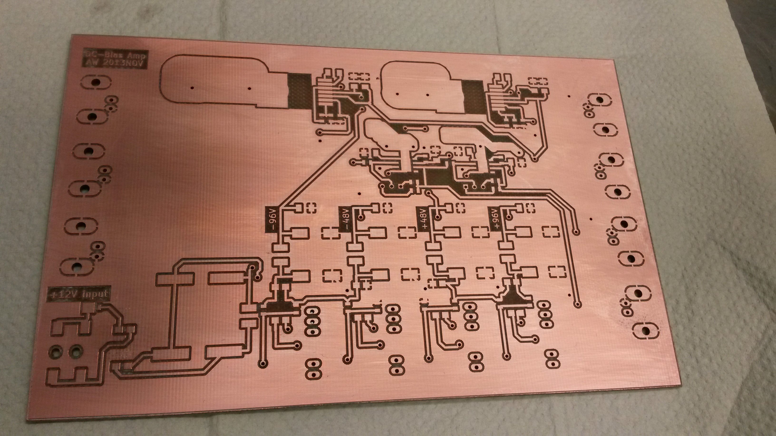
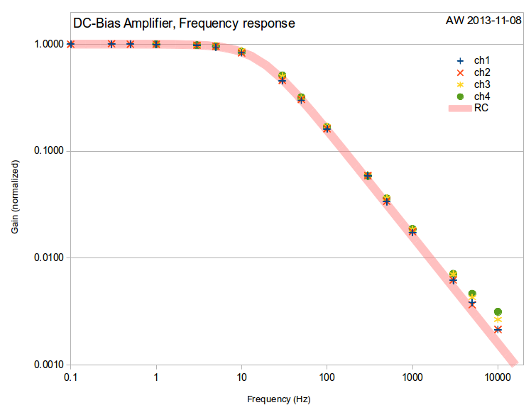
I've put together the first version of a DC-bias amplifier used for applying four DC-voltages to the trim electrodes of an ion trap. The axial voltages required are low, and they are applied symmetrically as +Vz and -Vz. The transverse voltages (X and Y) however can be as high as 100 V. Two high-voltage op-amps PA340CC are used for the X and Y channels, while the -Z and +Z output voltages are produced by two OPA454 op-amps. The amplifier has three +/-10 V inputs (Vx, Vy, Vz), and produces four outputs designed to be 10*Vx, 10*Vy, -Vz, and +Vz.
The amplifier circuit itself is very simple with the two PA340CC's in non-inverting configuration with a gain of 10, and the two OPA454's in inverting configuration, connected in series, with a gain of 1. The bandwidth requirement is very low, and the load should be equivalent to an open circuit - hence high 100k output resistor and a cap producing a 16 Hz low-pass filter on the output
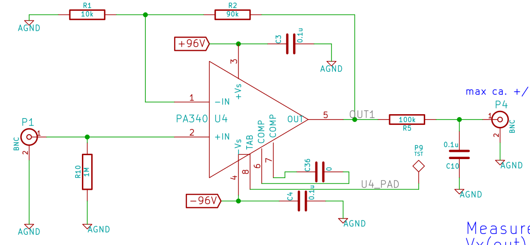
See full schematic as PDF: bias_amp_v0
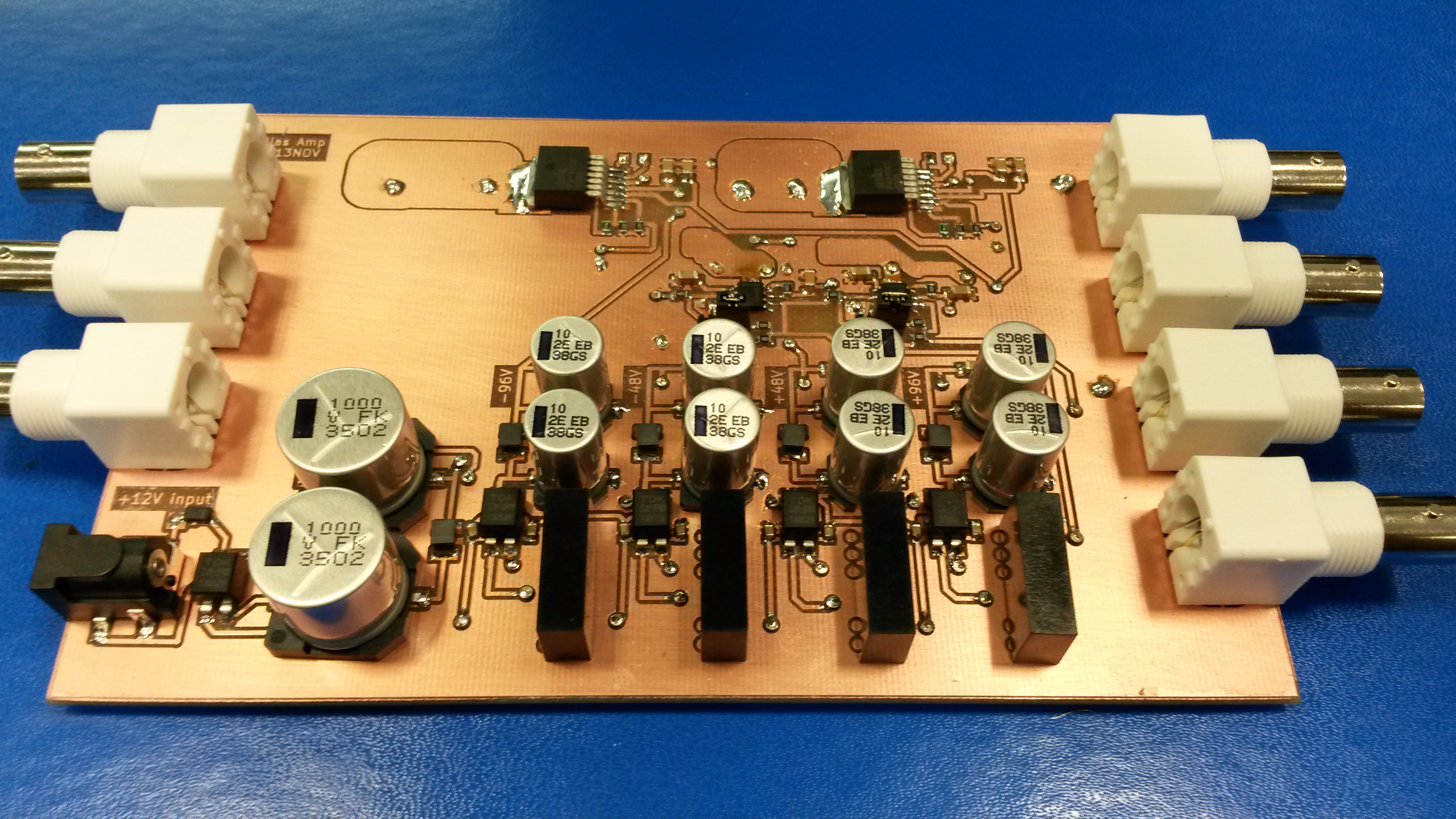
The high-voltage DC-rails for the op-amps are produced by connecting four +/-24 V DC-to-DC converters in series. This allows powering the amplifier from a single +12VDC powersupply-brick, and in theory produces +/-48 V for the lower-voltage op-amps and +/-96 V for the high-voltage op-amps.
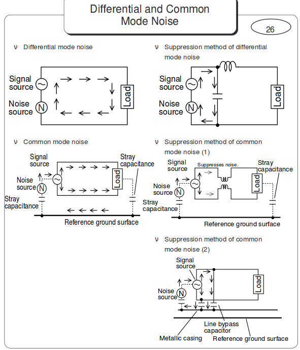
One issue with DC-to-DC converters is that they produce both differential and common-mode noise on the output. Conventional filter-caps or Pi-filtering removes the differential noise but does nothing to the common-mode noise. A common mode choke and/or filtering capacitors across the isolation-barrier to the input-side ground are required to remove the common-mode noise. Here's a picture from a Murata app-note that explains the idea:
The components fit comfortably on a 100mm by 160mm PCB like this:
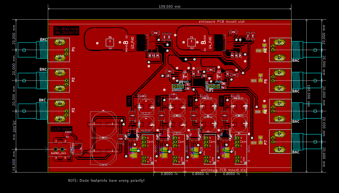
Only top Cu-layer shown. Why doesn't Kicad have built-in PDF export for the PCB-editor (like in the schematic-editor)?
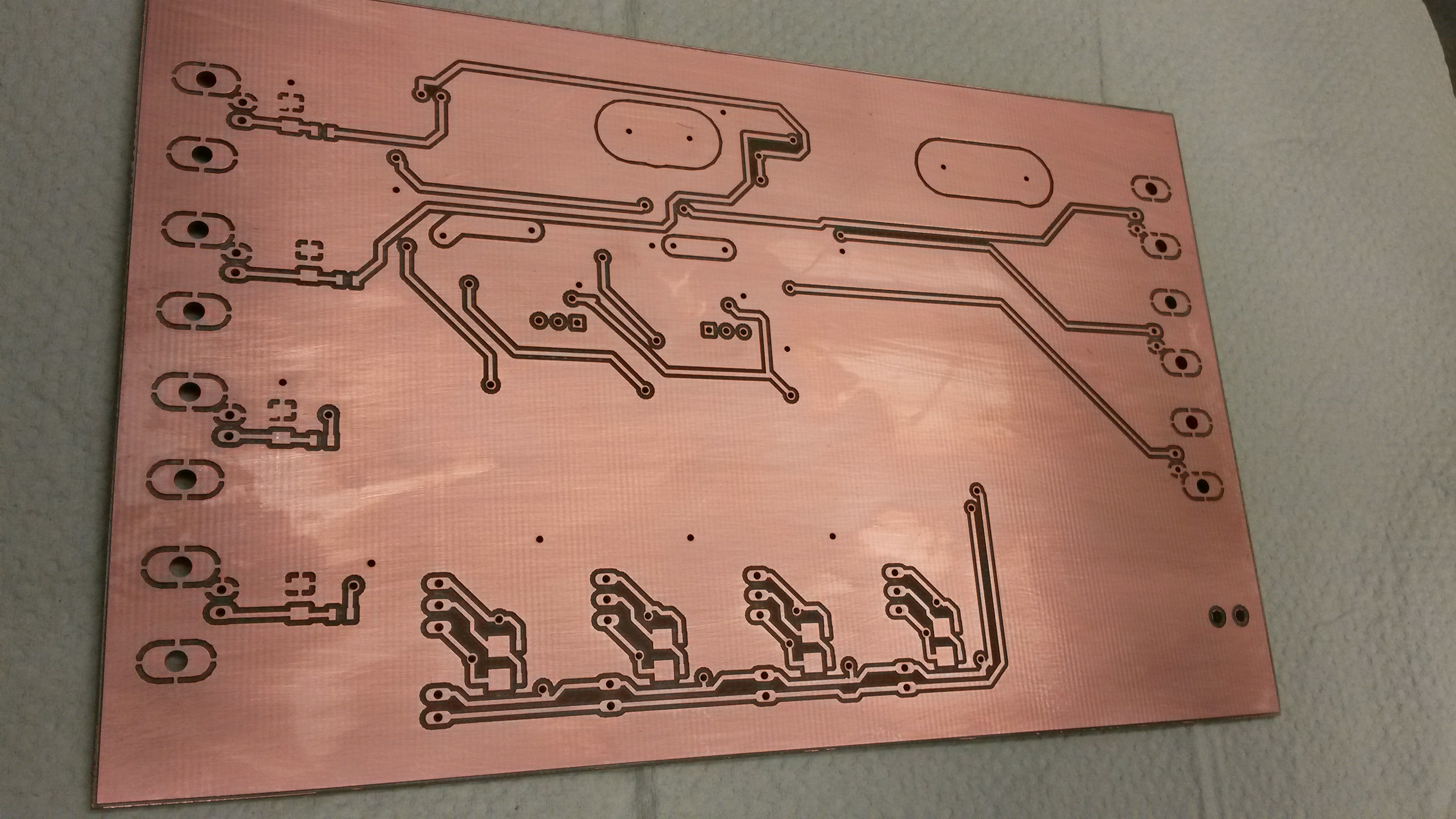
Gerber and Excellon files from Kicad worked without problems with CircuitCAM for producing toolpaths for BoardMaster that runs our LPKF PCB mill. The PCB after milling, rubbed with steel-wool, cleaned with isopropanol, and then coated with PRF202.
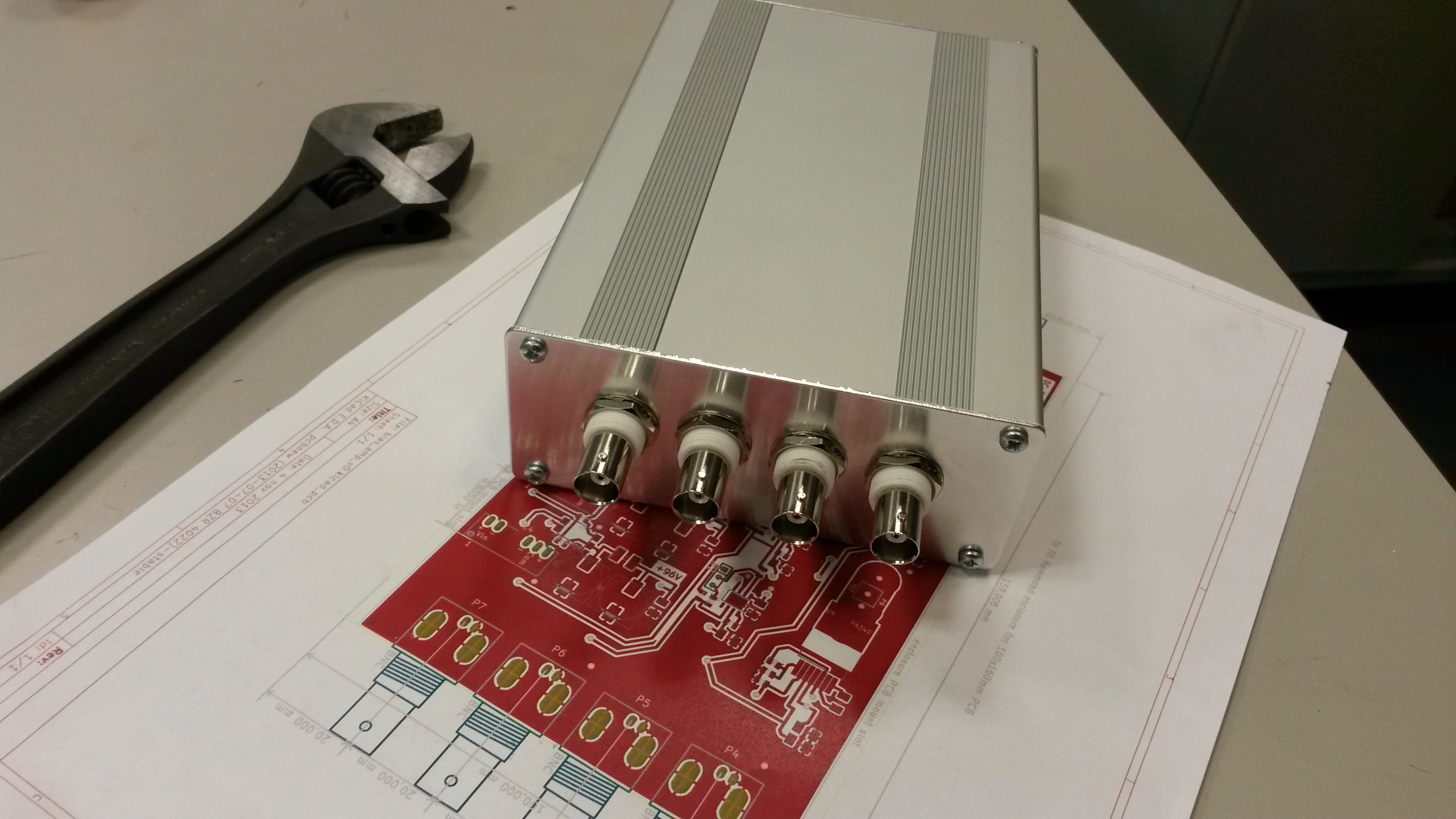
Components soldered, and board fit into an enclosure (Multicomp MCRECS160):
When powered up the DC-rails measured slightly lower voltages than expected. I got -89V, -44V, +44V, and +89V. The no-load input current was surprisingly high at 190mA. The dc-to-dc converters have a no-load spec of 20mA, so this explains about half of the measured current. The op-amps have a quiescent current of 3.2 mA @ +/48V for OPA454 and 2.2 mA @ +/-96V for PA340. So the 'middle' DC-to-DC converters that power all four op-amps should have 2*(3.2+2.2)= 10.8mA load at 48V and the 'side' converters only 2*3.2=6.4mA at 48V. That's 17.2 mA at 48V together, which should correspond to 84 mA at 12V if we trust the 82% efficiency number from the datasheet. So we can explain 80mA as no-load current and 84 mA from the quiescent current of the op-amps. That's 164 mA together, which is about 85% of the 190mA number shown by the powersupply. If my reasoning here is way off please comment below!
Initial measurements shows that the outputs behave roughly as designed. The high-voltage outputs max out at about +/- 85 V. Note that the 10 MOhm input of a DMM measures only 99% of the actual output voltage, due to the high 100k output impedance of the amplifier.
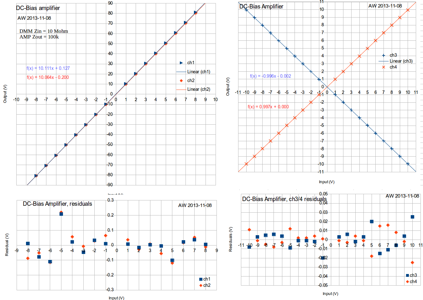
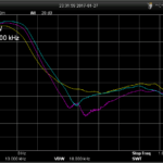
The frequency response is completely dominated by the 16 Hz low-pass RC-filter on the output, although the op-amps have unity-gain bandwidths of ~10 and ~2 MHz.
Notes and comments:
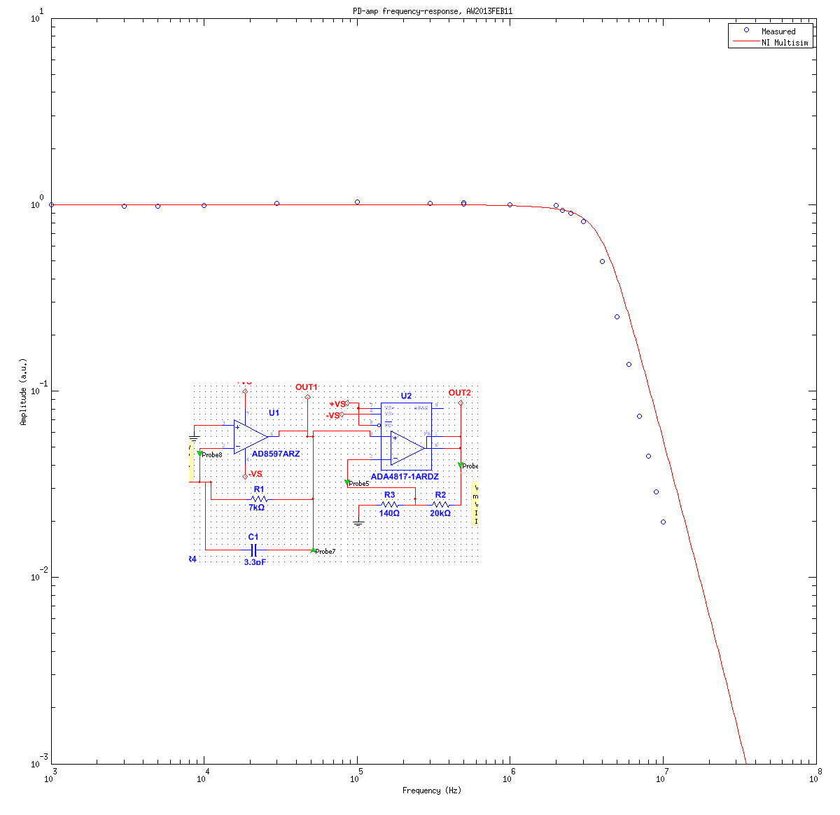
I assembled and tested the latest photodiode-amp today. I tested the frequency response using a red LED driven directly by an Agilent function-generator with an offset of 1.2 V and a 600 mVpp sine-wave. The LED datasheet doesn't specify a rise-time or bandwidth, but I'm hoping it is fast enough to test this 2-3 MHz receiver. I do have some small VCSELs that should be very fast and suitable for testing photodiode receivers up to 500 MHz and beyond.
The signal from the LED caused a 3 V output swing, which explains the slightly lower observed (large-signal) bandwidth compared to the simulated (small-signal) bandwidth. Some of the difference between the simulated frequency-response and the measured one is probably explained by stray capacitance which slightly lowers the bandwidth.
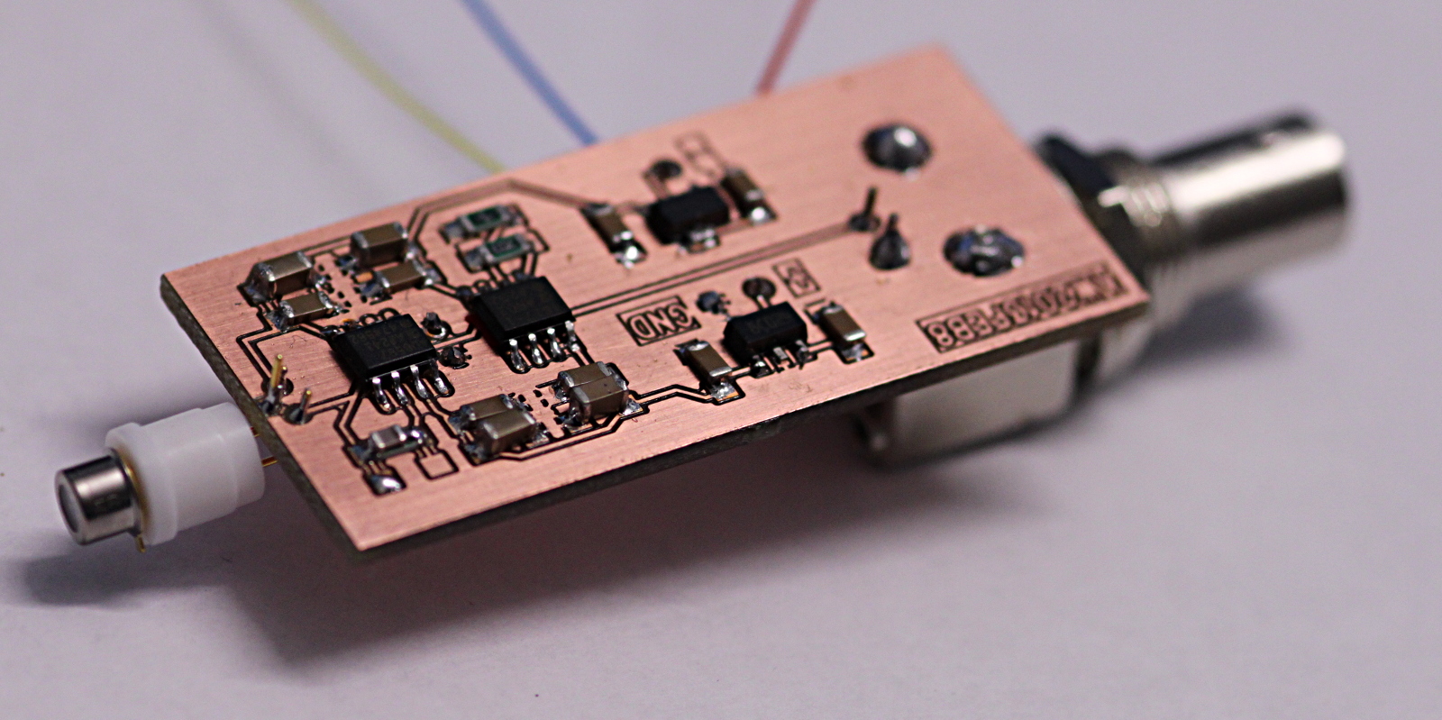
A revised version of the circuit and PCB for a photodiode amplifier, to be used in PDH-locking (Pound-Drever-Hall) as well as RAM-nulling (residual amplitude modulation) in a laser experiment I am doing. The changes compared to the first prototype are:
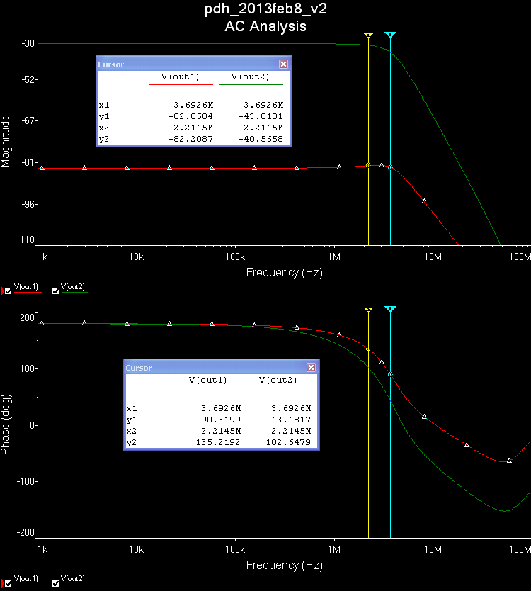
Here is a schematic and simulation results produced with the free version of NI Multisim from Analog Devices. The design is for roughly 1 MOhm of transimpedance gain in total, here split between 7 kV/A transimpedance gain, and 144 V/V for the non-inverting second op-amp. At 1 kV/A of transimpedance gain a 5 uW optical signal at 633 nm (HeNe laser!) that produces a 2 uA photocurrent will result in a 2 V output signal. The AC analysis shows very slight gain-peaking for the transimpedance-stage (red trace) and a -3 dB bandwidth of >3 MHz overall (green trace).
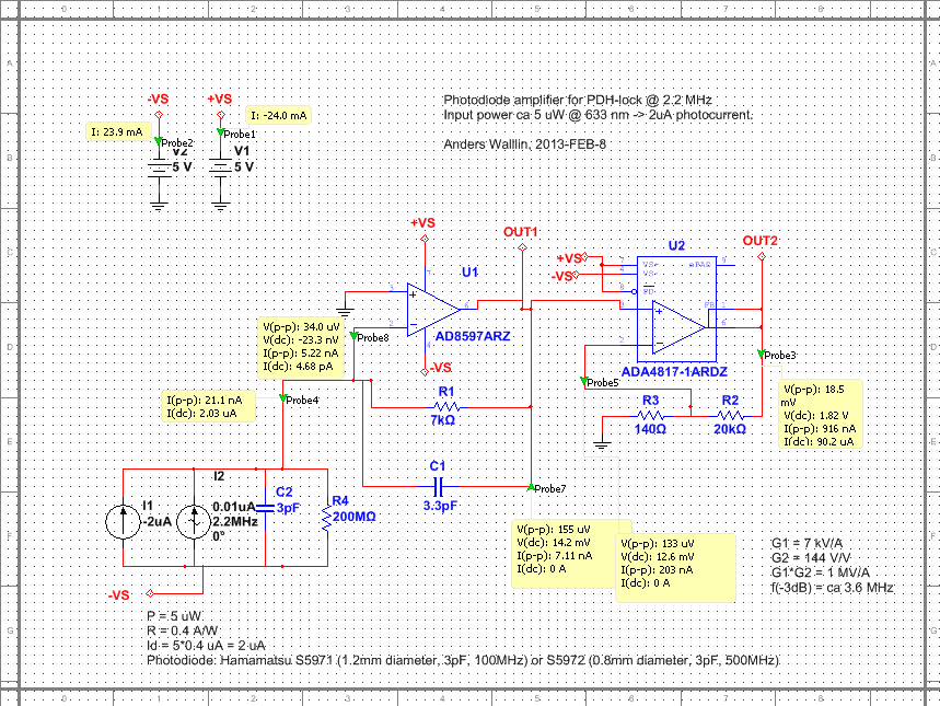
The first op-amp used in the transimpedance stage only needs to have a bandwidth slightly exceeding the transimpedance gain bandwidth (the feedback resistor R1 together with the compensating cap C1, the capacitance of the photodiode C2, and the input-capacitance (not shown) of the op-amp form an RC low-pass filter). The AD8597 is marketed as "ultralow distortion/noise" and is fast enough (10 MHz). The second non-inverting op-amp needs a high gain-bandwidth-product (GBP) since we are amplifying ~100-fold here. The ADA4817 has a small-signal bandwidth of 1 GHz and GBP~400 MHz, so should work OK here.
A voltage of only 14 mV over the transimpedance-resistor is not ideal. The Johnson noise (which in principle a good designer can control/minimize) in the resistor will dominate over the shot noise (which we cannot avoid) in the optical signal. For shot-noise limited performance the rule of thumb is to make the voltage drop at least 51 mV (which will make Johnson and shot noise equal). Without tricks however that is not possible as here we have both a weak signal (2 uA of photocurrent), we want a high gain (1 kV/A in total), and we want to go fast (~3 MHz bandwidth)! If you relax any of those requirements (more power, less gain, slower response) it is straightforward to build a shot-noise limited amplifier in one or two stages.
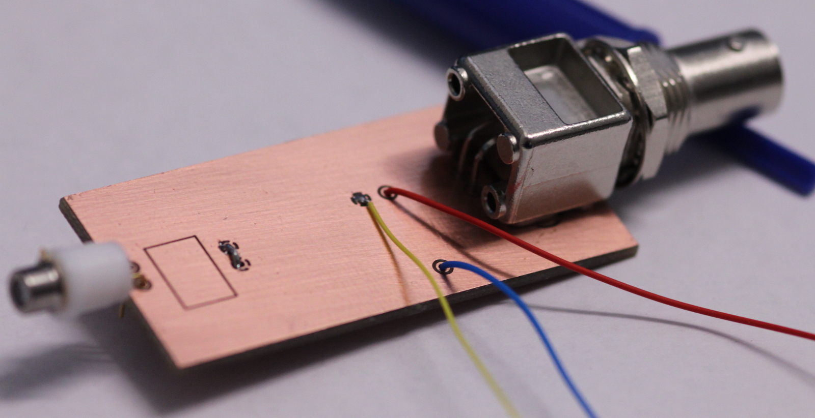
The PCB, fresh from the mill:
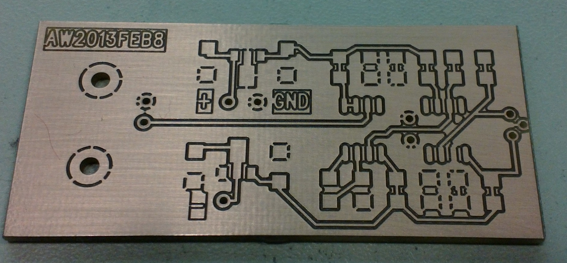
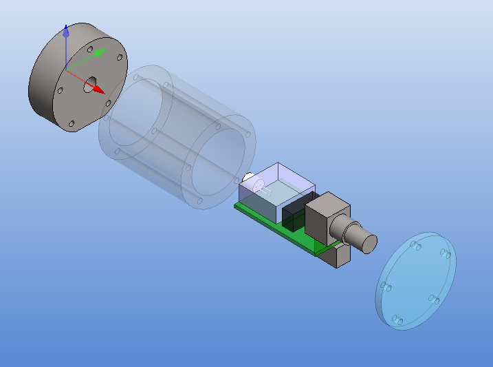
Far right is a 3-pin TO-18 socket for the photodiode. Right-middle are the two op-amps with their feedback-resistors/caps, as well as two de-coupling caps for both +5V and -5V. Left-middle are 7805 and 7905 voltage regulators, and the BNC output-connector is far left. All the surface mount components are mounted on the top layer of the board, while the through-hole components are bottom-mounted. Resistors and caps are 1206-size. This PCB should fit the earlier enclosures I turned on the lathe.
Hopefully I will have time to assemble and test one or two of these next week. I should measure the actual frequency-response and compare it with the simulated one.