250MHz detector with Fermionics FD80FC photodiode

Here's anoter one-inch-photodetector with a Fermionics FD80FC photodiode and 5k1 transimpedance. Bandwidth around 250 MHz. Predicted dark noise and frequency response with TIASim. The Fermionics diode has a capacitance of only 0.4 pF (80 um diameter active area), giving slightly better bandwidth than a Thorlabs FGA01FC (2 pF capacitance, 120 um diameter active area).

200MHz photodetector with OPA818, FGA01FC InGaAs photodiode, and RF=4k7

Here's another one-inch-photodetector using OPA818 with a 2pF@5V InGaAs fiber-coupled photodiode FGA01FC. With a transimpedance gain of 4k7 Ohms the bandwidth is just over 200 MHz. A TIASim model predicts the dark-noise and response reasonably well with a parasitic capacitance (over RF) adjusted to ca 0.12 pF. The spectrum-analyzer settings weren't ideal for looking at the dark-noise which should go down to the thermal-noise of the 4k7 resistor (dashed line) - but here the instrument noise-floor prevents us from seeing that.

400+ MHz photodetector with OPA818

One-Inch-Photodetecor in Thorlabs 1" mount. LT3093 negative-rail voltage regulator at the top, and LT3042 positive rail voltage regulator bottom right. OPA818 op-amp bottom center, with BUF602 output-driver bottom left.

After a number of failed attempts (with HMC799, OPA859), here is a reasonably fast One Inch Photodetector using OPA818, a FDS015 photodiode, and 1.2 kOhm transimpedance. Bandwidth is above 400 MHz, with the dark-noise and frequency-response in reasonable agreement with TIASim predictions.

With the detector blocked there's quite a lot of electrical feed-through with just the spectrum-analyzer TG-output on (see blue data points, especially above 1 GHz). I tried to correct for this roughly, shown as the orange data points.

Photodetector signal and noise

For the simple 'one-inch-photodetector' with a Hamamatsu S5973 photodiode, OPA657 op-amp, and 10 kOhm feedback-resistor the predicted noise-floor and signal output is fairly easy to compute, from a simplified schematic like this:

The photodiode is modeled as a current-source and adds some source-capacitance (in addition to the op-amp input capacitance). The board and components have some parasitic capacitance over RF, and additionally CF is chosen large enough for stability (no self-oscillation). A 50-ohm series resistor couples the signal into a coax to the spectrum-analyzer or scope.

For some (yet unknown..) reason I need to dial-down the GBWP of the op-amp to about half the datasheet value of 1.6 GHz - only then do I get good agreement between the predicted and measured spectra:

Note y-axis units in dBm/RBW with RBW=10kHz. Siglent SSA3000X spectrum analyzer, preamp on.

Ideally we'd want the dark-noise to be close to the thermal/Johnson noise of RF (like it, roughly, is at <10 MHz), but the circuit has a noise-peak as the -3dB bandwidth is approached. The 'bright' detector response was measured by shining light from a VCSEL onto the detector and modulating the laser with the TG output from the spectrum analyzer. Moving the divergent laser source closer or further away from the detector adjusts the signal level.

Here is the same plot with linear frequency scale.

One Inch Photodetector, v1

Here's a transimpedance amplifier board that fits inside a 1" lens-mount. It has low noise LDOs (LT3042 and LT3094) and a SOT-23-6 op-amp footprint (for e.g. OPA657 or OPA847).

The first board has a S5973 photodiode, an OPA657, a 10 kOhm feedback resistor, and a 0.2pF feedback capacitor. The circuit self-oscillates without any feedback capacitor.

The backside of the board has an MMCX-connector for the output signal, and 3 wires for power supplies (max +/-20V).

The noise-floor shows an ~18 dB bump as the 59 MHz -3dB bandwidth is approached - not that great. At low frequencies the noise-floor agrees with the thermal noise of a 10k resistor. Shot-noise from about 10uW optical power, producing a 4 uA photocurrent (photodiode responsivity ~0.4A/W), should be clearly (3 dB or so) above the 10k resistor thermal noise floor.

The noise-bump could be decreased with a larger feedback-capacitor, but this reduces bandwidth. The source capacitance is due to the S5973 photodiode (1.6 pF) and the differential (0.7 pF) and common-mode (4.5 pF) input-capacitance of the OPA657 op-amp. Clearly a lower input-capacitance opamp would be better. Stay tuned for tests with OPA858...

Note to self: can't use the Siglent SA's default detector mode of "Positive-peak" if we want quantitative dBm numbers from the analyzer. Use "sample" detector mode!

PD-Amp v.2 assembled and tested

pd_amp_smd-side_2013feb11 pd_amp_thruhole-side_2013feb11

I assembled and tested the latest photodiode-amp today. I tested the frequency response using a red LED driven directly by an Agilent function-generator with an offset of 1.2 V and a 600 mVpp sine-wave. The LED datasheet doesn't specify a rise-time or bandwidth, but I'm hoping it is fast enough to test this 2-3 MHz receiver. I do have some small VCSELs that should be very fast and suitable for testing photodiode receivers up to 500 MHz and beyond.

The signal from the LED caused a 3 V output swing, which explains the slightly lower observed (large-signal) bandwidth compared to the simulated (small-signal) bandwidth. Some of the difference between the simulated frequency-response and the measured one is probably explained by stray capacitance which slightly lowers the bandwidth.

pd_amp_f-response_2013feb11_withcircuit_x


Photodiode amplifier - version 2

A revised version of the circuit and PCB for a photodiode amplifier, to be used in PDH-locking (Pound-Drever-Hall) as well as RAM-nulling (residual amplitude modulation) in a laser experiment I am doing. The changes compared to the first prototype are:

  • The required bandwidth and gain is not easy to achieve in one stage, so there's a second stage of amplification after the transimpedance amplifier.
  • I'm suspicious of the noise caused by the switched-mode powersupply, as well as the DC2DC converter, of the previous design. So this circuit has just +/-5 V regulators and can be driven from a regular (known good) +/-12 V lab powersupply (or even two 9 V batteries).

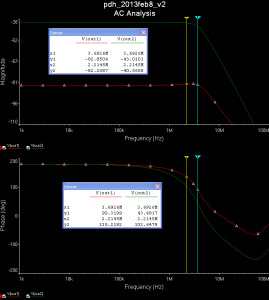
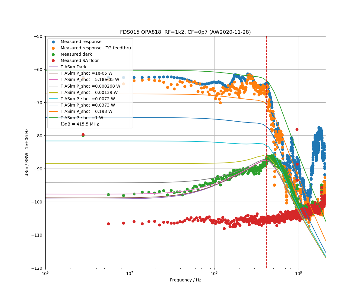
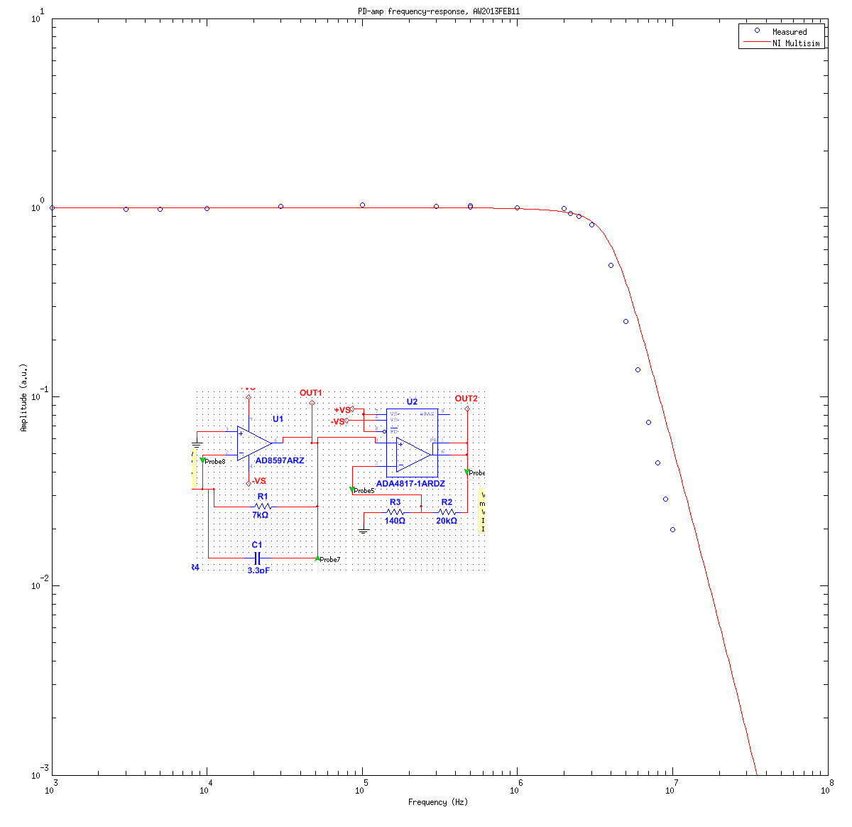
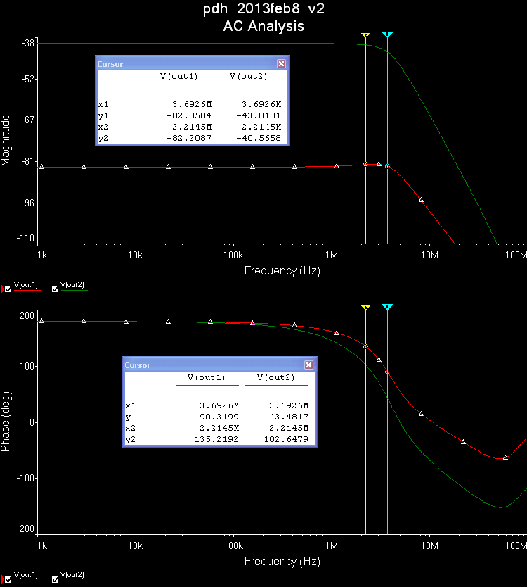
Here is a schematic and simulation results produced with the free version of NI Multisim from Analog Devices. The design is for roughly 1 MOhm of transimpedance gain in total, here split between 7 kV/A transimpedance gain, and 144 V/V for the non-inverting second op-amp. At 1 kV/A of transimpedance gain a 5 uW optical signal at 633 nm (HeNe laser!) that produces a 2 uA photocurrent will result in a 2 V output signal. The AC analysis shows very slight gain-peaking for the transimpedance-stage (red trace) and a -3 dB bandwidth of >3 MHz overall (green trace).

pd_amp_2013feb8 pd_amp_2013feb8_ac_sim

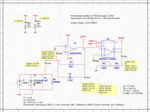
The first op-amp used in the transimpedance stage only needs to have a bandwidth slightly exceeding the transimpedance gain bandwidth (the feedback resistor R1 together with the compensating cap C1, the capacitance of the photodiode C2, and the input-capacitance (not shown) of the op-amp form an RC low-pass filter). The AD8597 is marketed as "ultralow distortion/noise" and is fast enough (10 MHz). The second non-inverting op-amp needs a high gain-bandwidth-product (GBP) since we are amplifying ~100-fold here. The ADA4817 has a small-signal bandwidth of 1 GHz and GBP~400 MHz, so should work OK here.

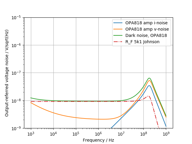
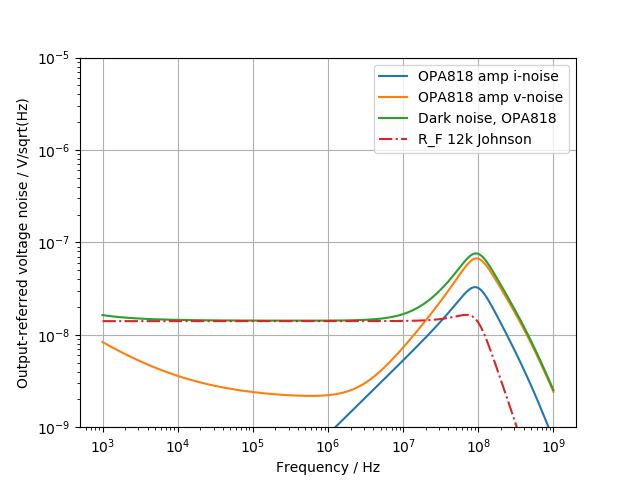
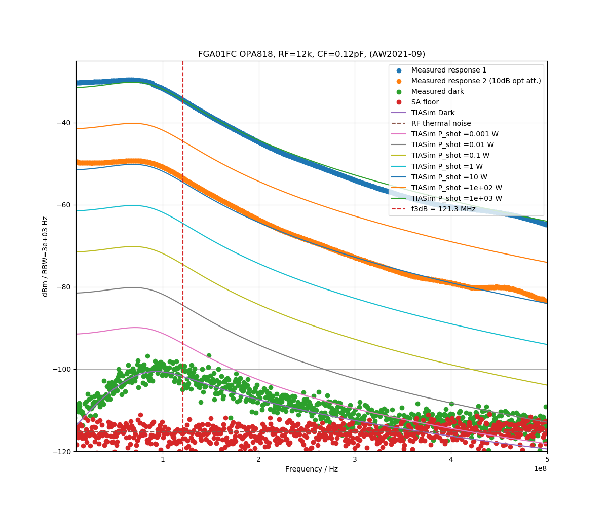
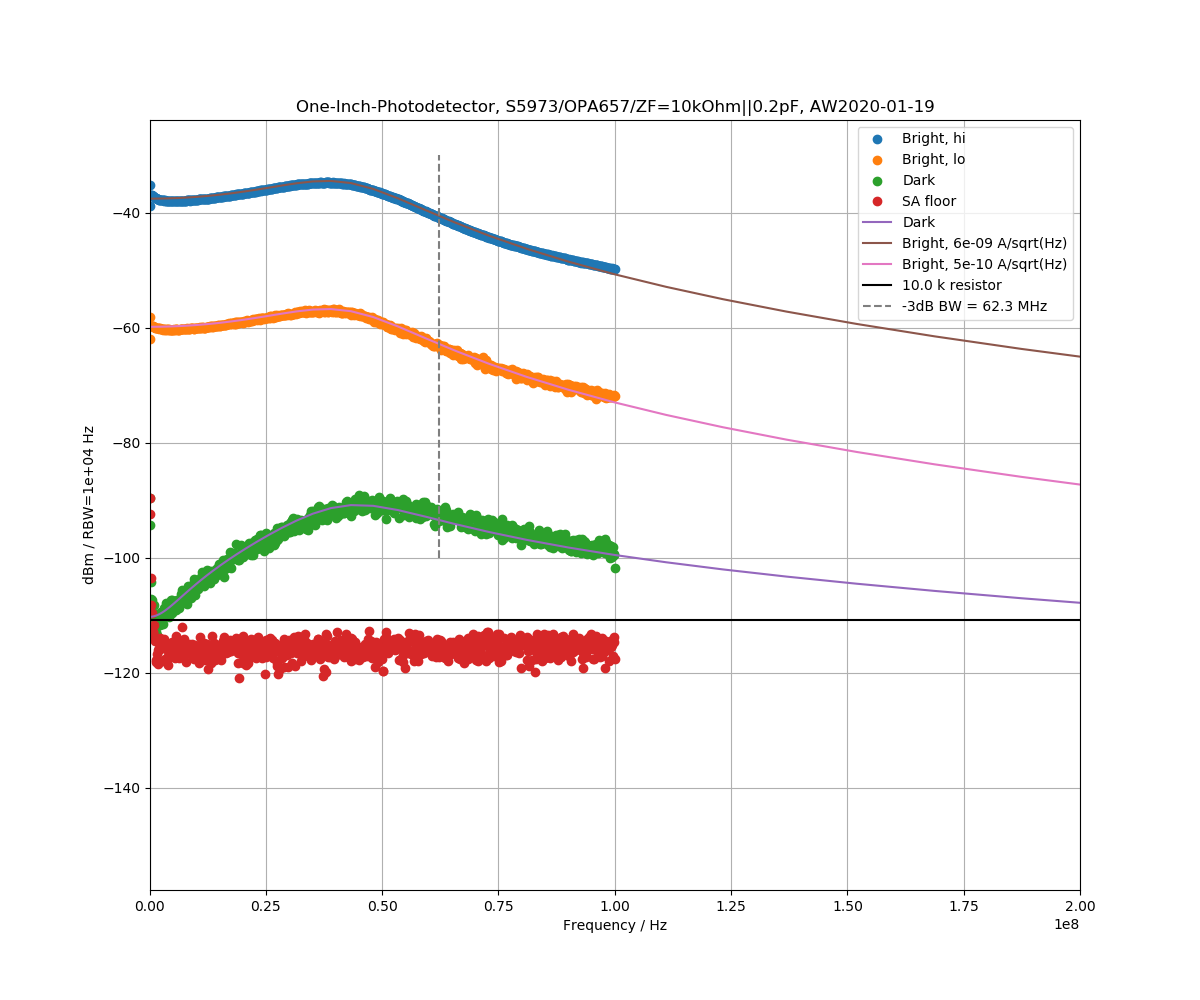
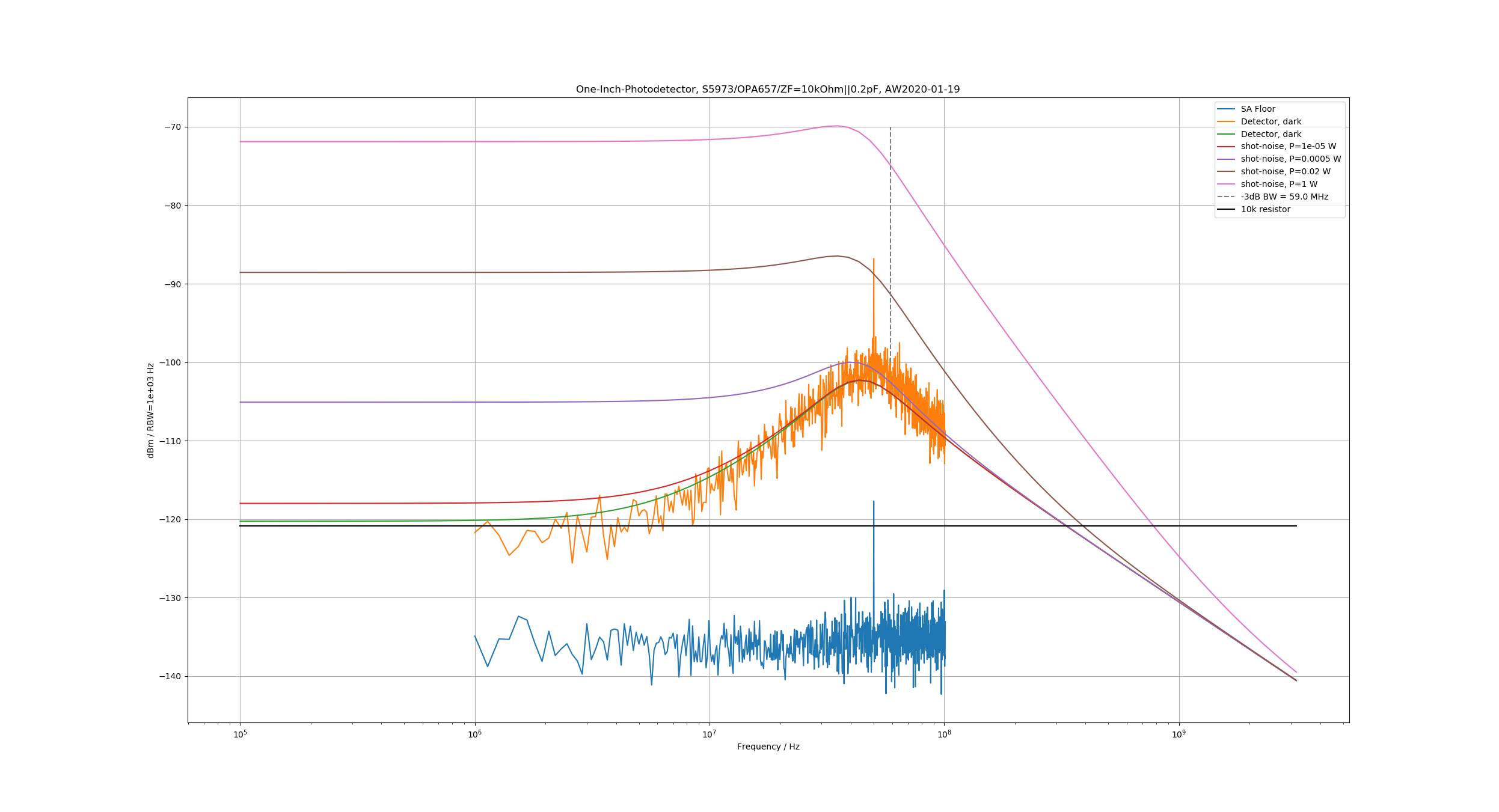
A voltage of only 14 mV over the transimpedance-resistor is not ideal. The Johnson noise (which in principle a good designer can control/minimize) in the resistor will dominate over the shot noise (which we cannot avoid) in the optical signal. For shot-noise limited performance the rule of thumb is to make the voltage drop at least 51 mV (which will make Johnson and shot noise equal). Without tricks however that is not possible as here we have both a weak signal (2 uA of photocurrent), we want a high gain (1 kV/A in total), and we want to go fast (~3 MHz bandwidth)! If you relax any of those requirements (more power, less gain, slower response) it is straightforward to build a shot-noise limited amplifier in one or two stages.

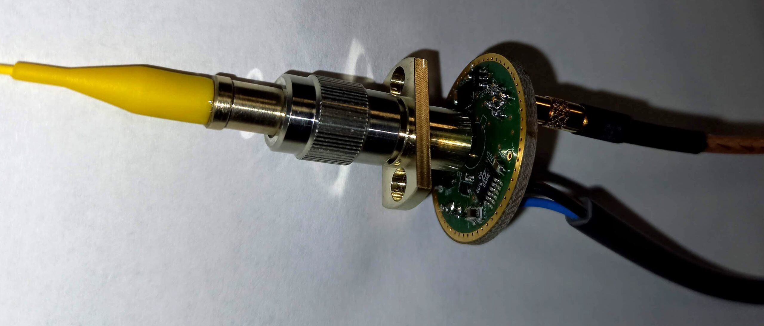
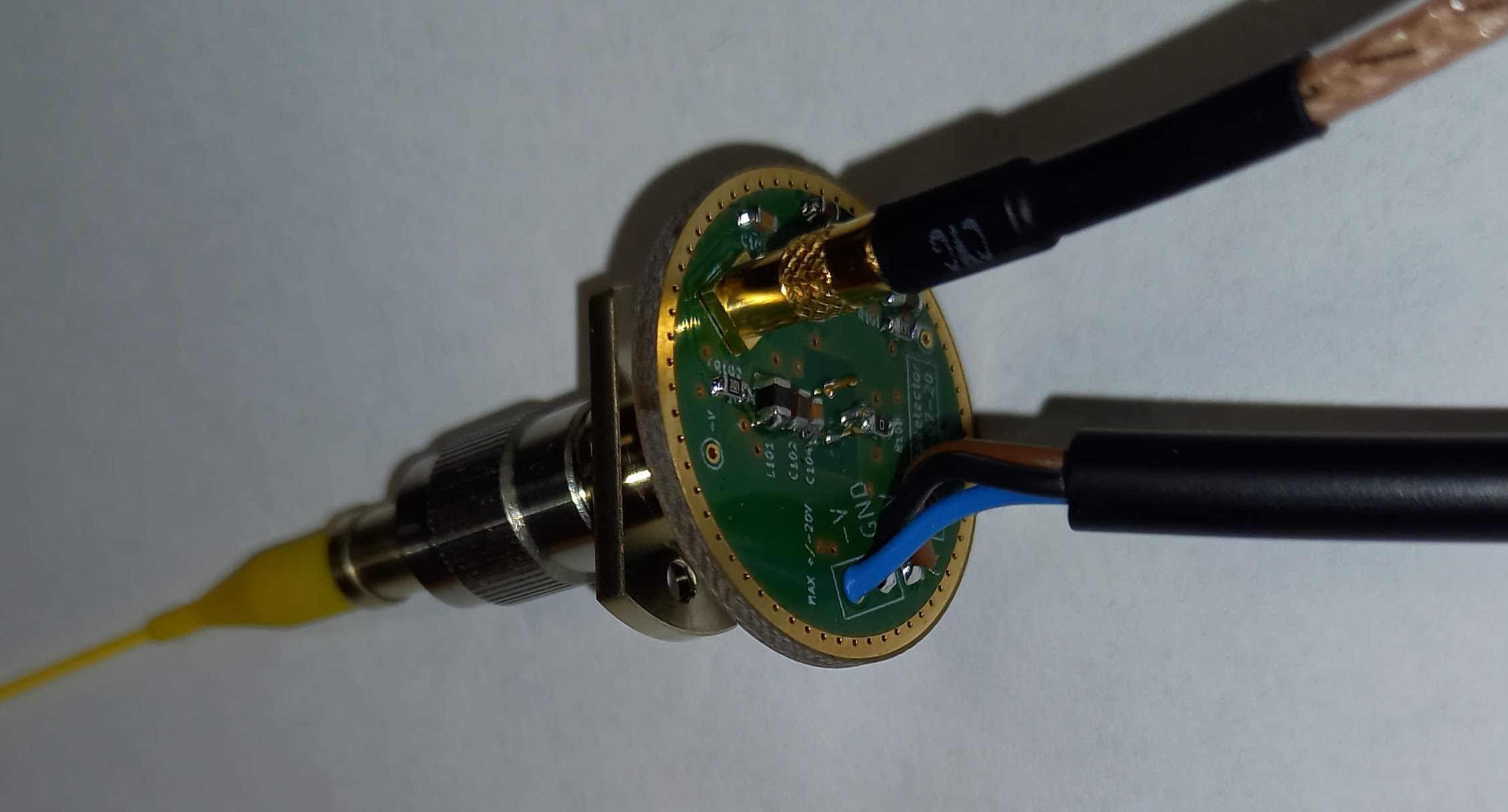
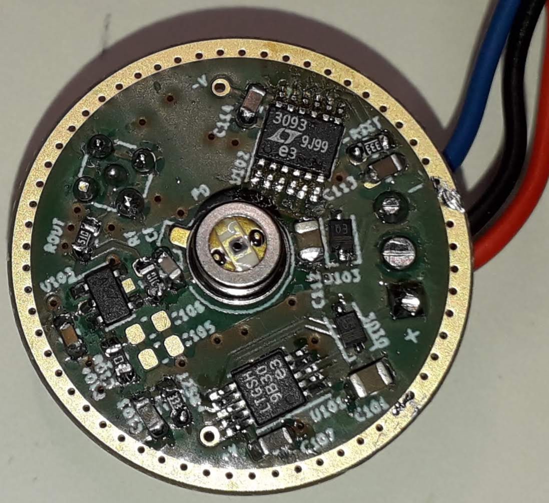
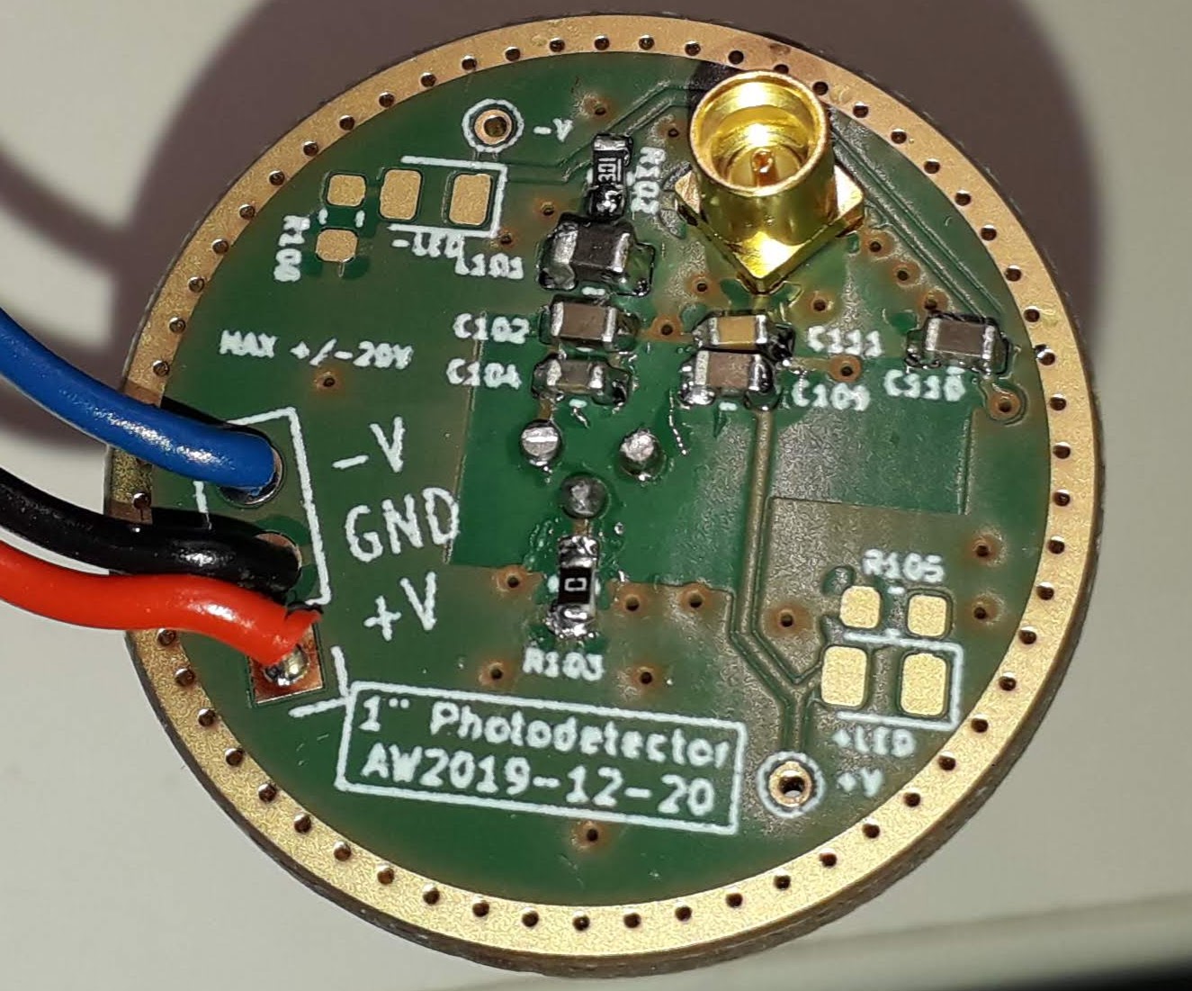
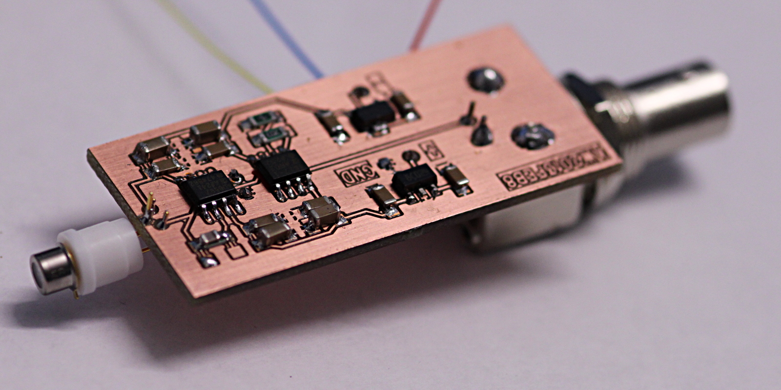
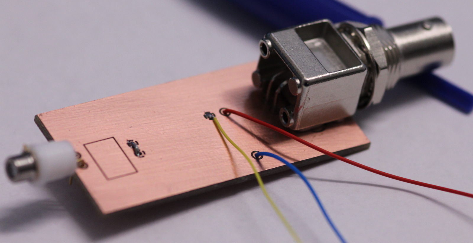
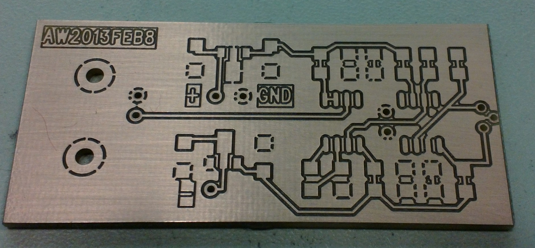
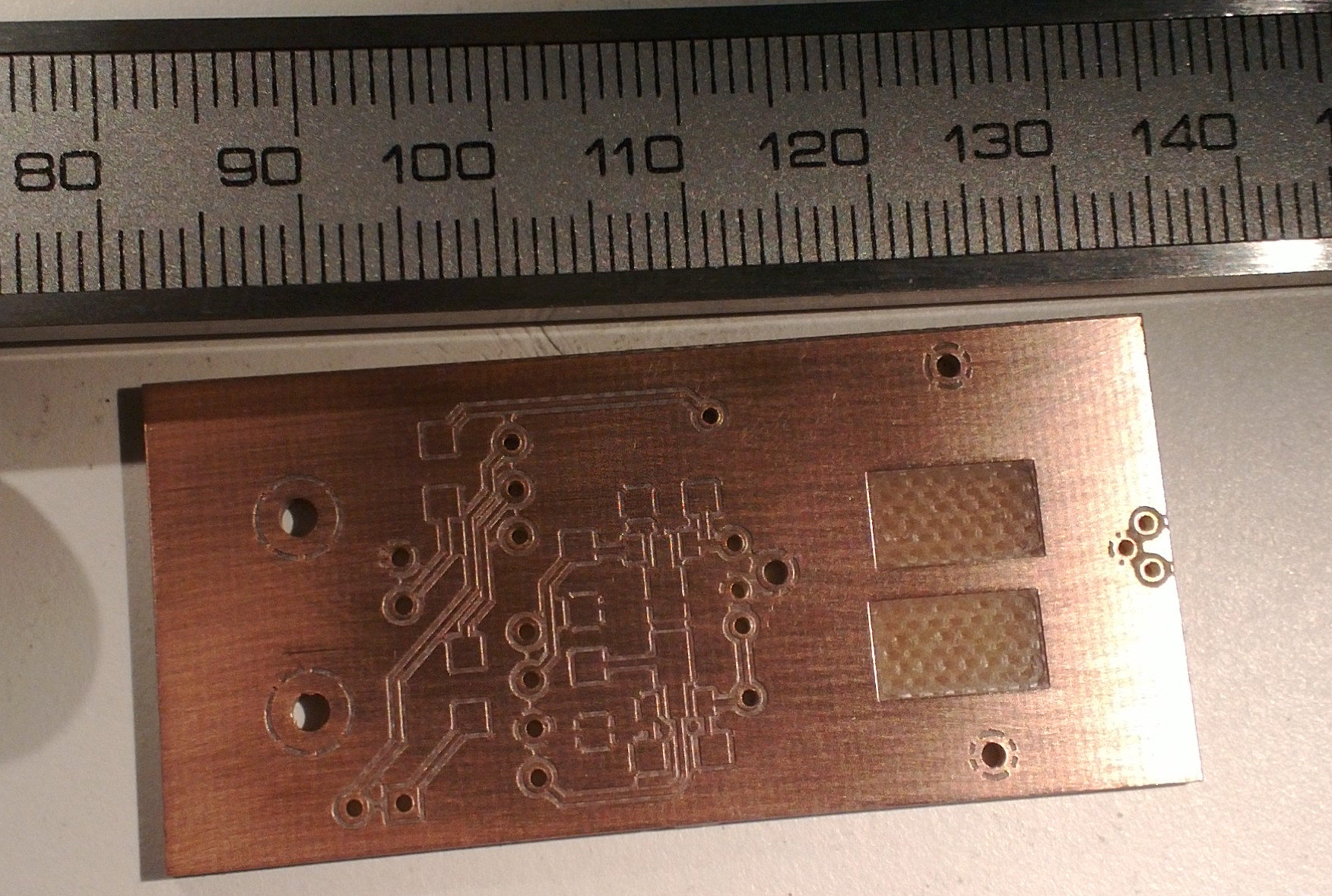
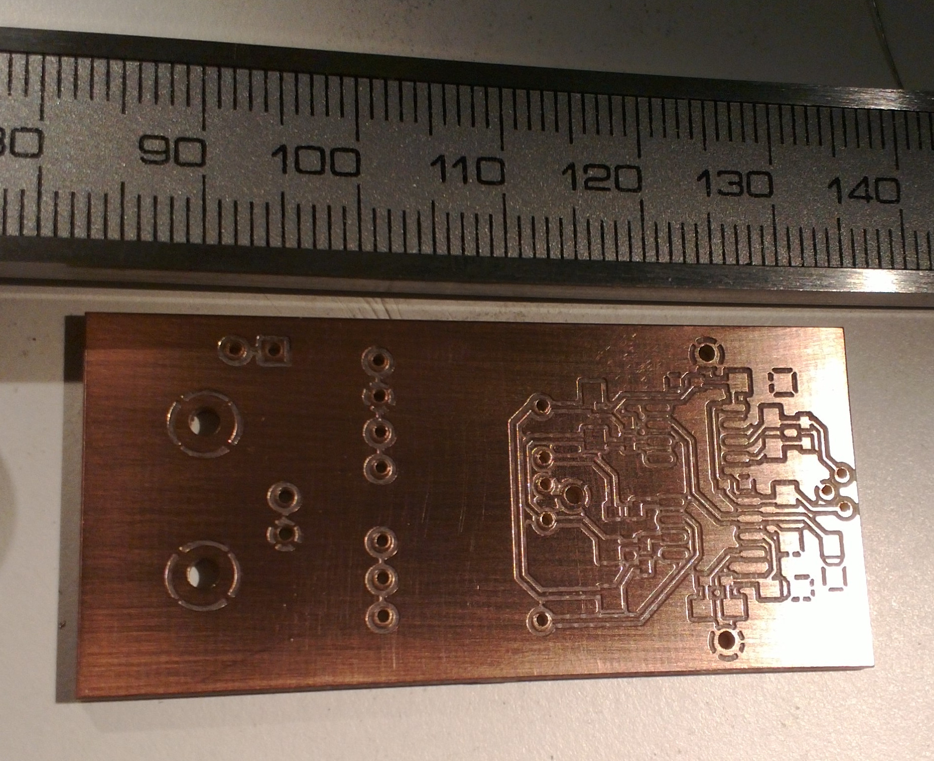
The PCB, fresh from the mill:

pd_amp_pcb_2013feb8

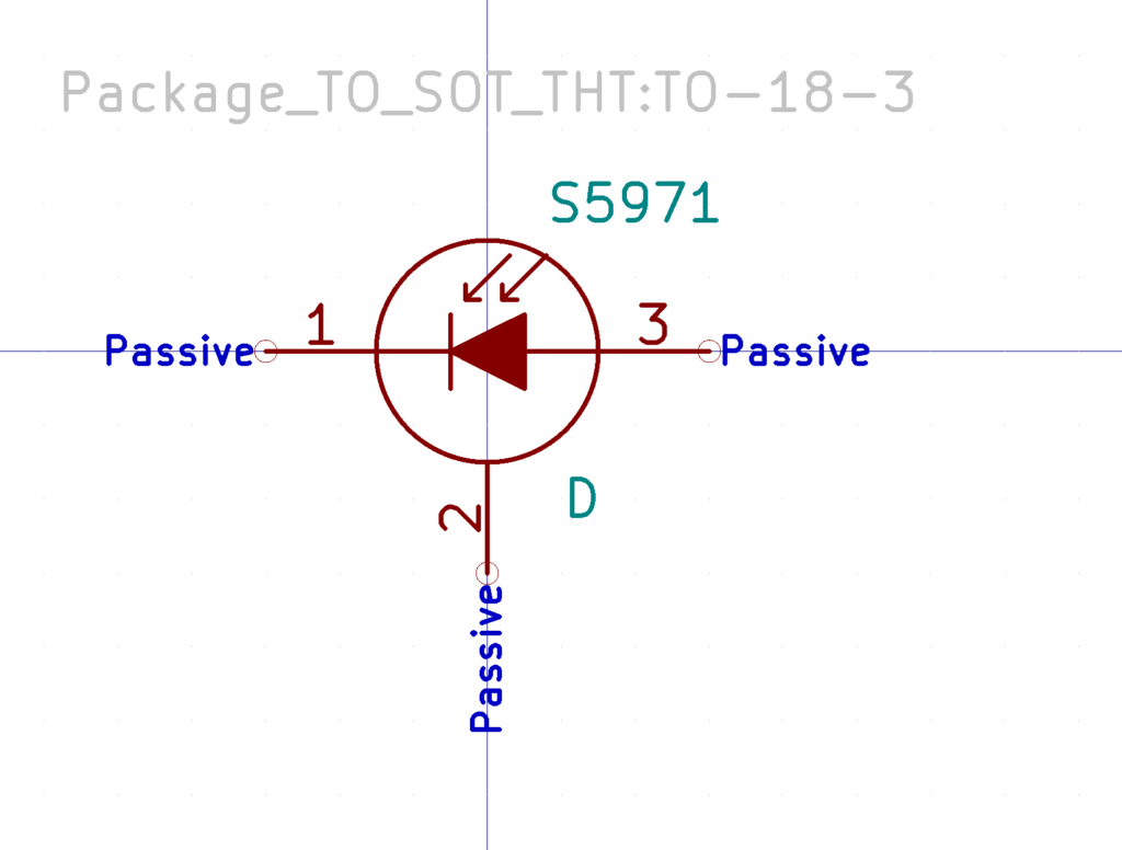
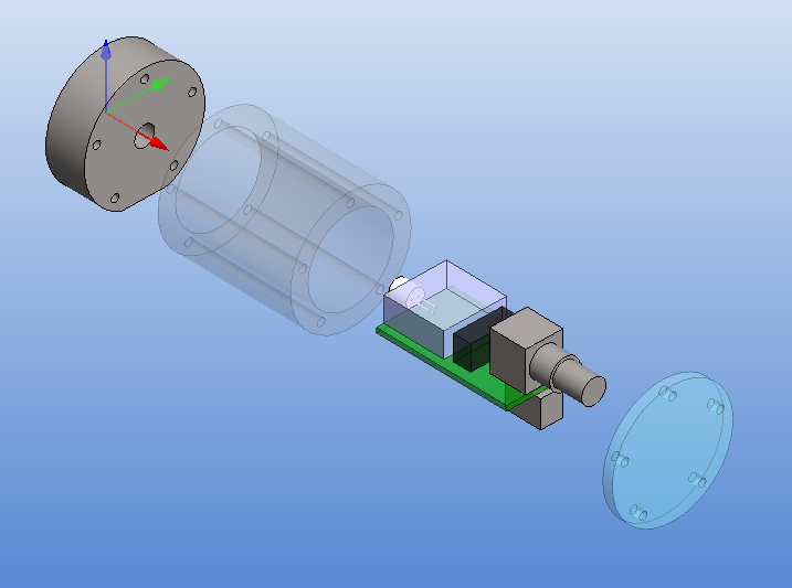
Far right is a 3-pin TO-18 socket for the photodiode. Right-middle are the two op-amps with their feedback-resistors/caps, as well as two de-coupling caps for both +5V and -5V. Left-middle are 7805 and 7905 voltage regulators, and the BNC output-connector is far left. All the surface mount components are mounted on the top layer of the board, while the through-hole components are bottom-mounted. Resistors and caps are 1206-size. This PCB should fit the earlier enclosures I turned on the lathe.

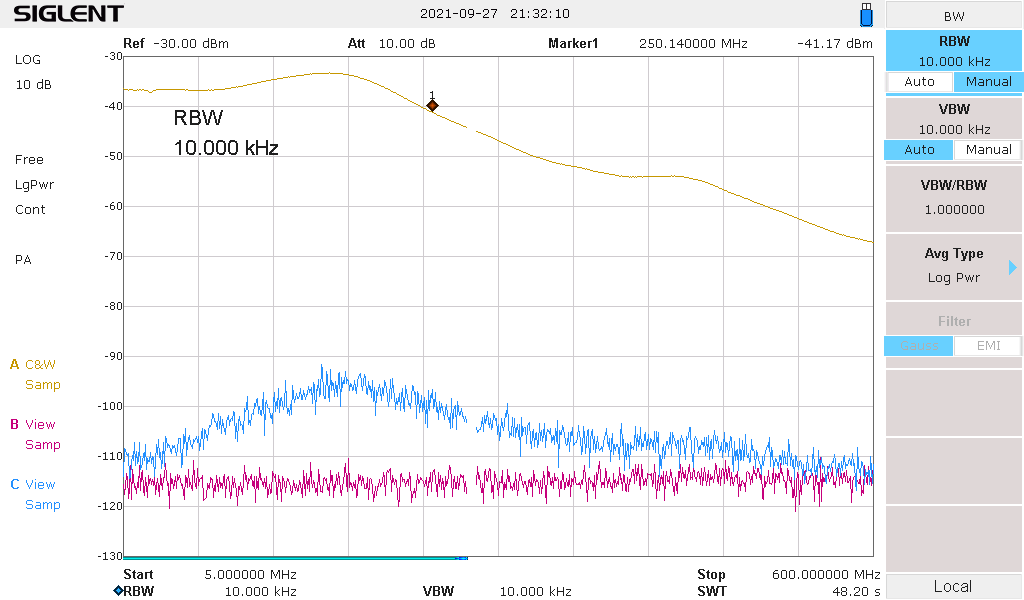
Hopefully I will have time to assemble and test one or two of these next week. I should measure the actual frequency-response and compare it with the simulated one.

A second photodiode amplifier PCB

I made this PCB for a second photodiode amplifier today. This one is designed for higher light-levels and higher bandwidth. I will post the schematics along with measurement data when I've tested the circuit.

beat_amp_pcb_bottom beat_amp_pcb_top

The V-cutter is designed to cut a slot that is nominally 8 mils (0.2 mm) wide, but the actual cut-width depends on how the z-axis is adjusted. Removing the ground-plane copper from under the high-speed op-amps is supposed to minimize stray capacitance.