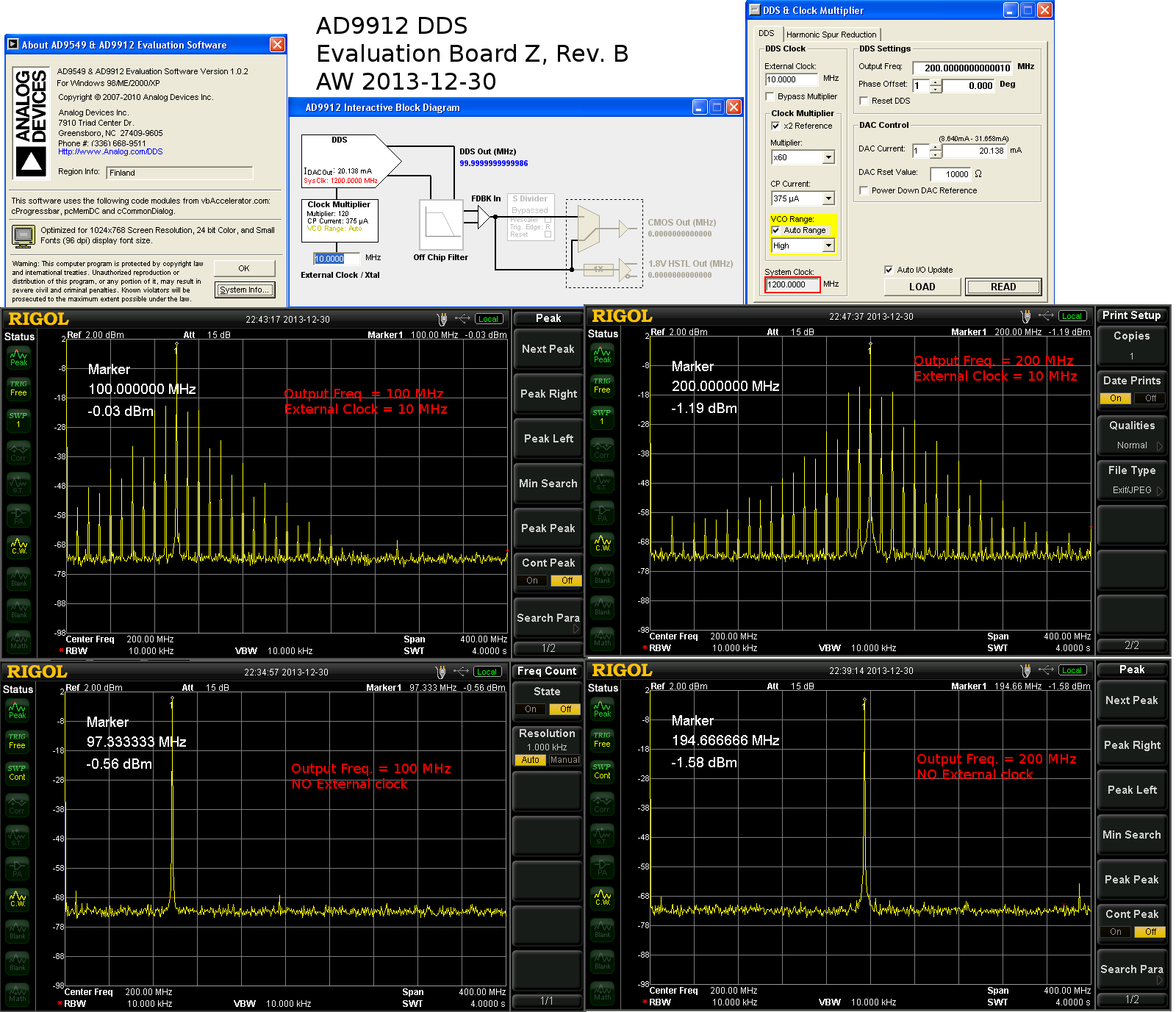
See also discussion on the AD forum: https://ez.analog.com/dds/f/q-a/107510/ad9912-ftw-lsb-always-zero
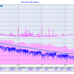
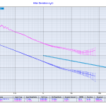
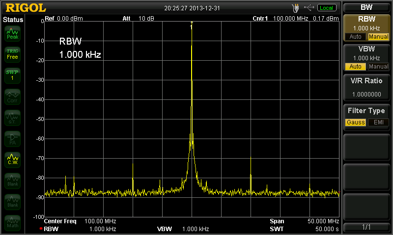
We've tried to measure the frequency resolution of the AD9912 DDS, which when used with a 1 GHz SYSCLK should be 1 GHz / 2**48 = 3.55 uHz.
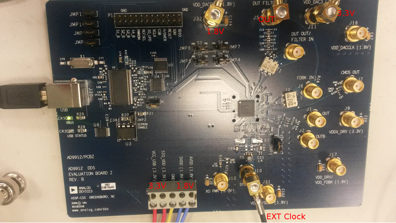
We tried an ARTIQ Urukul-board and an AD dev-board and got the following results:
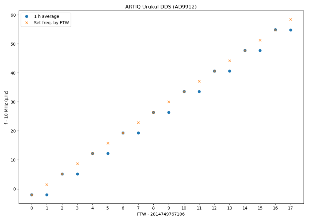
ARTIQ Urukul AD9912 DDS output frequency vs. FTW 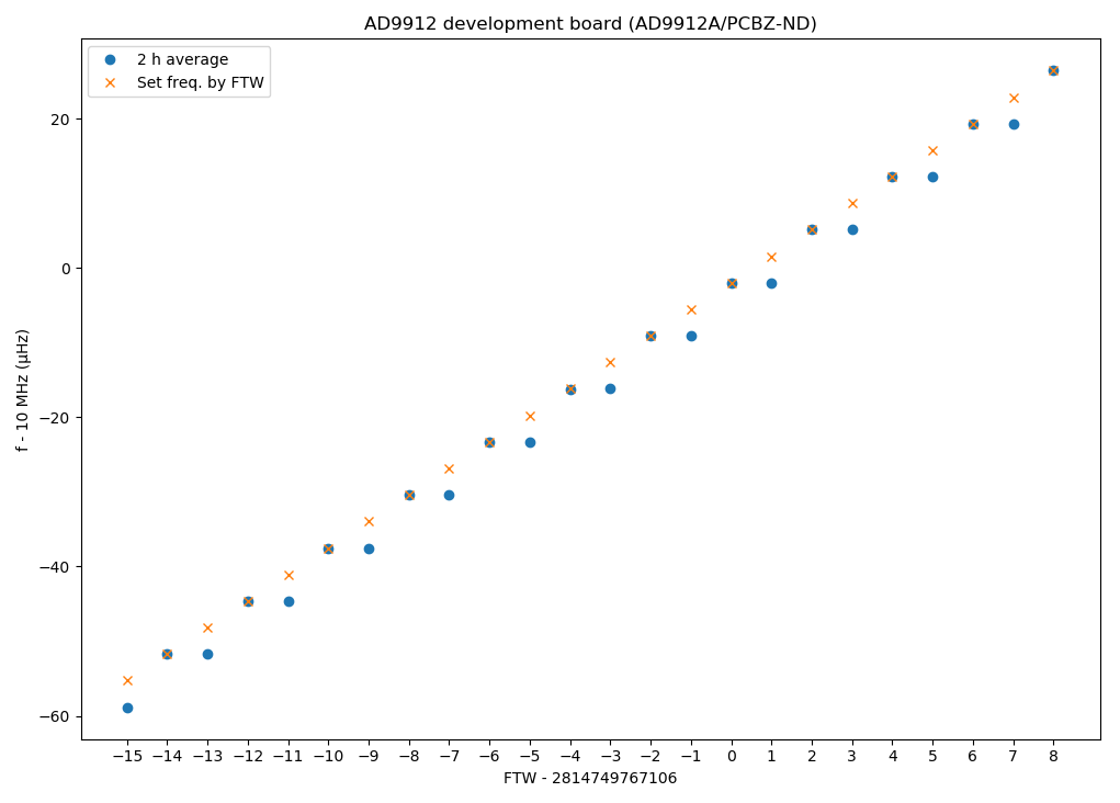
AD9912 dev-board output frequency vs. FTW
In both cases the output frequency corresponds to an even frequency tuning word (FTW) although we step the frequency by one LSB. In other words the LSB appears to be zero in all cases, even when we write an odd FTW with '1' as the LSB. Instead of the expected 3.55 uHz frequency resolution we see double-sized steps of 7.1 uHz.
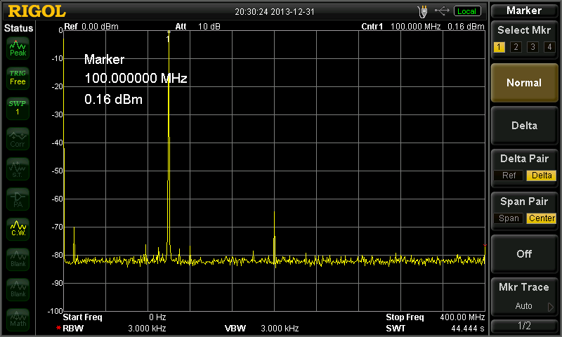
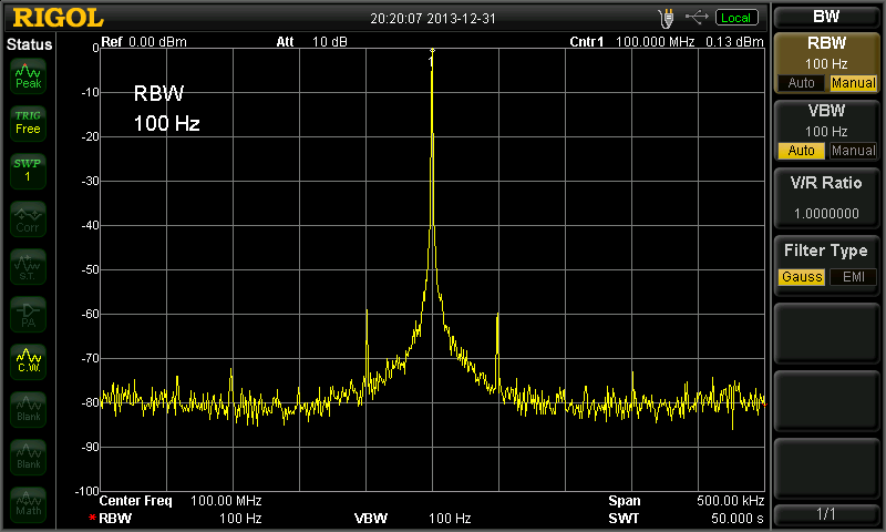
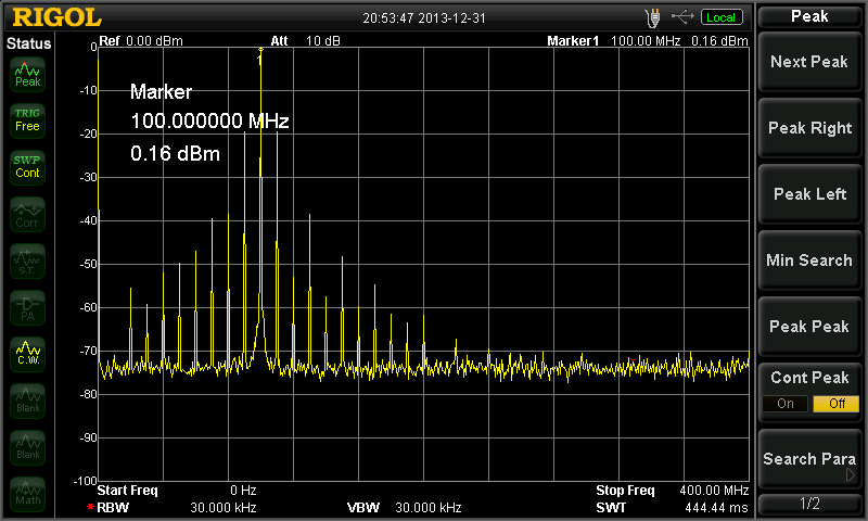
The Urukul measurement was done with a Microsemi 3120A phase-meter and the dev-board was measured using a PICDIV 1PPS-divider followed by a Keysight 53230A time interval counter. The even FTW frequencies agree with the predicted frequency to much better than 0.1 uHz.