A revised version of the circuit and PCB for a photodiode amplifier, to be used in PDH-locking (Pound-Drever-Hall) as well as RAM-nulling (residual amplitude modulation) in a laser experiment I am doing. The changes compared to the first prototype are:
- The required bandwidth and gain is not easy to achieve in one stage, so there's a second stage of amplification after the transimpedance amplifier.
- I'm suspicious of the noise caused by the switched-mode powersupply, as well as the DC2DC converter, of the previous design. So this circuit has just +/-5 V regulators and can be driven from a regular (known good) +/-12 V lab powersupply (or even two 9 V batteries).
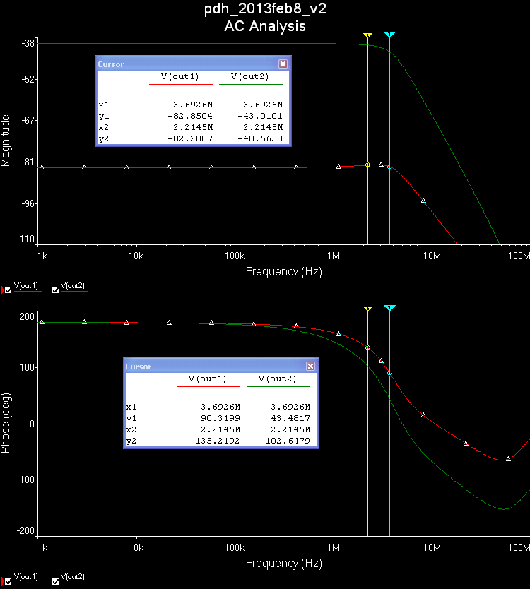
Here is a schematic and simulation results produced with the free version of NI Multisim from Analog Devices. The design is for roughly 1 MOhm of transimpedance gain in total, here split between 7 kV/A transimpedance gain, and 144 V/V for the non-inverting second op-amp. At 1 kV/A of transimpedance gain a 5 uW optical signal at 633 nm (HeNe laser!) that produces a 2 uA photocurrent will result in a 2 V output signal. The AC analysis shows very slight gain-peaking for the transimpedance-stage (red trace) and a -3 dB bandwidth of >3 MHz overall (green trace).
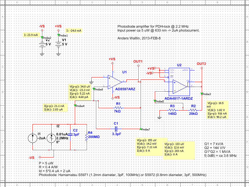
The first op-amp used in the transimpedance stage only needs to have a bandwidth slightly exceeding the transimpedance gain bandwidth (the feedback resistor R1 together with the compensating cap C1, the capacitance of the photodiode C2, and the input-capacitance (not shown) of the op-amp form an RC low-pass filter). The AD8597 is marketed as "ultralow distortion/noise" and is fast enough (10 MHz). The second non-inverting op-amp needs a high gain-bandwidth-product (GBP) since we are amplifying ~100-fold here. The ADA4817 has a small-signal bandwidth of 1 GHz and GBP~400 MHz, so should work OK here.
A voltage of only 14 mV over the transimpedance-resistor is not ideal. The Johnson noise (which in principle a good designer can control/minimize) in the resistor will dominate over the shot noise (which we cannot avoid) in the optical signal. For shot-noise limited performance the rule of thumb is to make the voltage drop at least 51 mV (which will make Johnson and shot noise equal). Without tricks however that is not possible as here we have both a weak signal (2 uA of photocurrent), we want a high gain (1 kV/A in total), and we want to go fast (~3 MHz bandwidth)! If you relax any of those requirements (more power, less gain, slower response) it is straightforward to build a shot-noise limited amplifier in one or two stages.
The PCB, fresh from the mill:
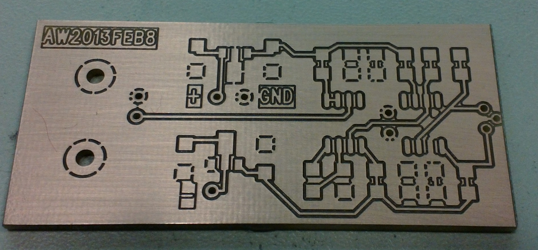
Far right is a 3-pin TO-18 socket for the photodiode. Right-middle are the two op-amps with their feedback-resistors/caps, as well as two de-coupling caps for both +5V and -5V. Left-middle are 7805 and 7905 voltage regulators, and the BNC output-connector is far left. All the surface mount components are mounted on the top layer of the board, while the through-hole components are bottom-mounted. Resistors and caps are 1206-size. This PCB should fit the earlier enclosures I turned on the lathe.
Hopefully I will have time to assemble and test one or two of these next week. I should measure the actual frequency-response and compare it with the simulated one.
I would like to know how you set up your instrumentation to measure the gain bandwidth of the photodiode amplifier that was designed here. I am designing a similar device using Texas instruments OPT101 and I would like to simulate the circuit and the gain bandwidth in using National Instruments Multisim version 11 S/W.
Hi Pete,
The simulation in Multisim or LTSpice will entirely depend on how good and realistic a SPICE model you find for the OPT101. Don't trust the simulator too much 🙂
With RF=1 MOhm the OPT101 has a bandwidth of only 14 kHz, which is quite easy to test.
The measurement idea is simple: use a modulated light source with a BW much higher than your photoreceiver, look at the photoreceiver output with an oscilloscope, and increase the frequency (e.g. in log steps) until you get enough data points for the bode-plot you want.
Almost any LED can be modulated up to a few MHz. Watch out for "white-light" LEDs as these have a blue LED with a phosphor coating. The phosphor is "slow" and will limit the bandwidth of the LED.
For quick tests you can drive the LED directly off the output of a signal generator (such as an Agilent 33120A or similar). The 50 ohm output impedance works as a current-limiting resistor 🙂
The signal generator can usually output a DC-offset of 1 or 2 V which will provide a DC-level of light output from the LED. On top of this just add a sine-wave with a suitable amplitude (100 mV or more ) and you should see a received sinewave on your photoreceiver output.
If you want a better circuit for driving the LED look for example here:
http://hyperphysics.phy-astr.gsu.edu/hbase/electronic/ledmod.html
You can ofcourse do this with a fancy spectrum-analyzer also. They usually have an output where you get a frequency-swept sine wave at say 0 dBm amplitude level, and the spectrum analyzer input which will automagically plot the frequency response on screen. Using a spectrum analyzer makes sense if you are aiming for ~100 MHz or more bandwidth.
hope this helps,
Anders
Anders,
After a few simulations it is apparent that neither the OPT 101 nor 301 is fast enough for our application. I will try to build your circuit in Multisim and achieve the same results, as we are looking for a detector with a 5MHZ bandwidth. One question, the circuit in the bottom left corner is the modeled photo diode correct? Is R4 part of the modelling , or is it separate from the diode? The current sources, is this how you are performing the AC analysis? How would the diode appear in the actual circuit? To achieve a larger bandwidth I would adjust C1 and R1 (f3dB=1/2PiC1R1)?
Thanks
Pete A
Hi,
Yes the components in the lower left corner model the photodiode.
The DC current source corresponds to a DC light level. The AC current source corresponds to modulated light incident on the photodiode.
Including the capacitance C2 of the photodiode is essential to get reasonable results. This scales with the area of the photodiode, so low capacitace fast photodiodes tend to be very small (100s of micrometers in diameter). A reverse bias voltage applied to the photodiode reduces this capacitance (but increases dark-current), and this is often used to increase the bandwidth.
The shunt resistance of the diode R4 is very large and will not have a big impact on the simulation. You can remove it and see how much the simulation changes.
Your formula for the bandwidth (f3dB=1/2PiC1R1) is correct if C1 is large compared to all other capacitances in the circuit. If you really want to push the bandwidth you need to take into account the photodiode capacitance as well as the op-amp input capacitance also (these are usually at least a few pF).
A 5 MHz bandwidth receiver, even shot-noise limited (51 mV or more over R1) is easy if you have a lot of light (milliWatts) incident on the photodiode, but could be quite challenging if you only have microWatts.
I hope to have time to do better write-up on the noise-sources and shot-noise at some point... I probably need to build one or two of these ~few MHz bandwidth 10-100 microWatt photodiode receivers in the near future so that might inspire more blogging.
Anders
Here's a picture of how a minimal photodiode receiver would look like:
http://electronics.stackexchange.com/questions/72540/how-do-i-connect-a-photodiode-detecting-laser
Note the reverse bias which is not shown in my simulation schematic.
In the simulation the current-sources, photodiode capacitance C2, and shunt resistance R4, all just model the photodiode.
Anders,
Thanks for the quick and informative reply. One last question, where did you get the Op-amp models for mulitsim? I found some amps, with similar characteristics, manufactured by Texas Instruments in the op-amp library. I am using Multisim 11.
Analog Devices has a version of NI Multisim downloadable from their site (free to use for one year, IIRC). That version includes lots of models for AD components.
Maybe you can install the AD-NI-Multisim version, and then export the components you need and import them into your Multisim 11?
Hello Anders,
In this post you mentioned that you were "...suspicious of the noise caused by the switched-mode powersupply, as well as the DC2DC converter..."
Did you verify if the DC2DC converter indeed introduced noise?
regards.
Hi Aris,
I didn't investigate the DC2DC converter any further.
The DC2DC will typically introduce both common-mode noise (same on both the GND and the +V output) as well as differential noise.
A common-mode choke can be used to suppress the common-mode noise.
My post over here has more info on the filtering:
http://www.anderswallin.net/2013/11/dc-bias-amplifier/
Anders