Some assembly of the PCB and enclosure for the first photodiode amplifier has happened today. Soldering the surface-mount components under a microscope was mostly easy - but trying to solder larger parts that require significant heating with the same tiny soldering iron used for small SMD parts was a mistake. The big parts were easy once I switched to a bigger soldering iron, but the BNC-connector was already a mess by then.
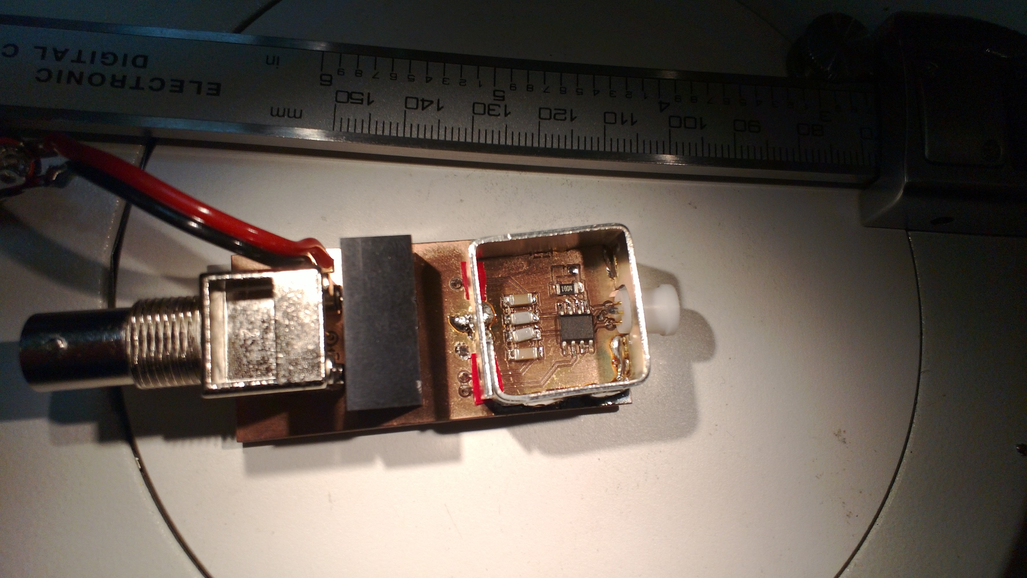
On the left a BNC connector. The black box in the middle is a DC-2-DC converter that produces +/-12VDC outputs from a single +9...18VDC input. The transimpedance amplifier on the right is based on an ADA4817 op-amp and is housed inside an RF screening can. On the far right is a white TO-18 socket for the photodiode.
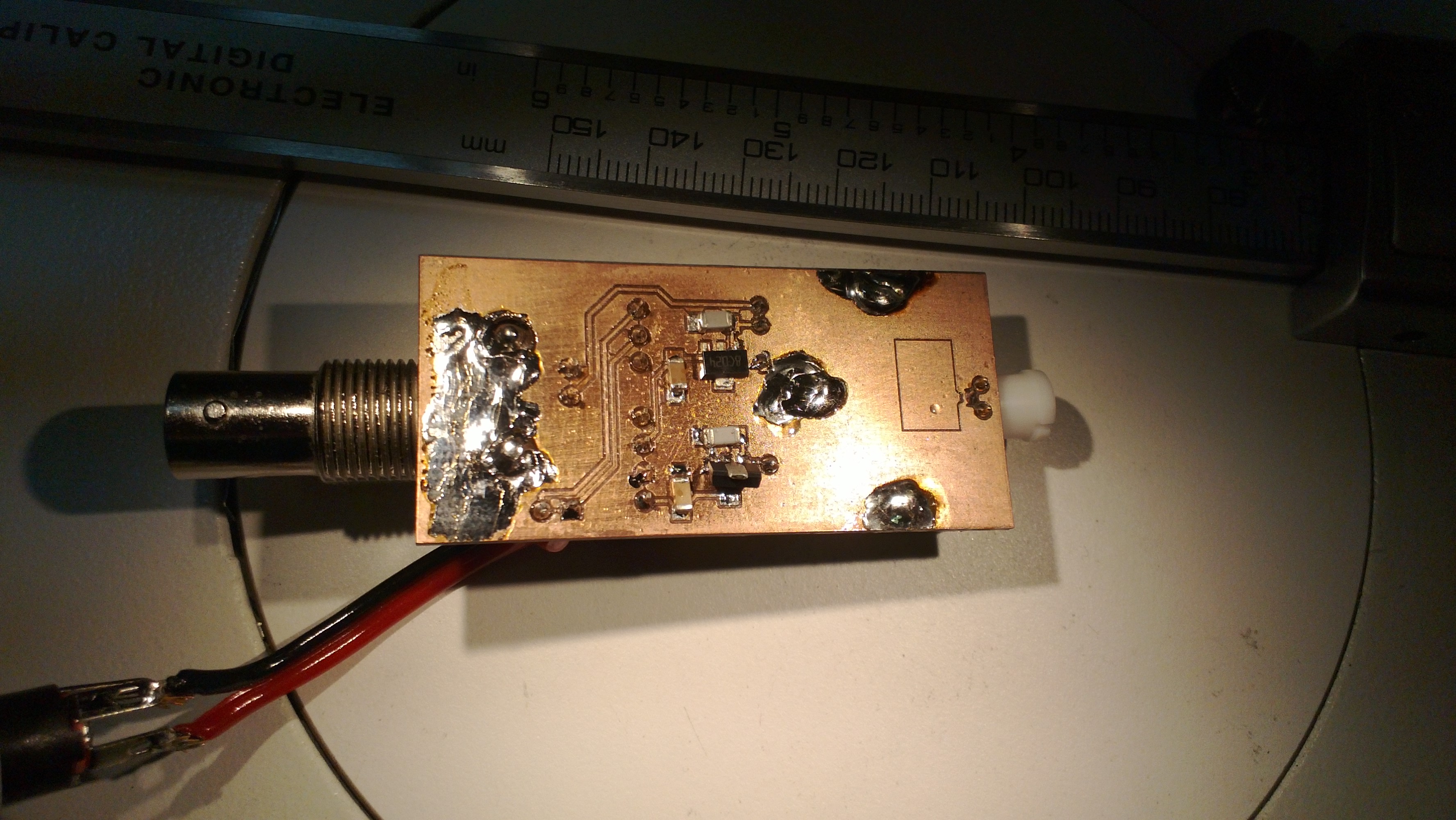
The underside of the board has 7805 and 7905 voltage regulators that produce stable (hopefully!) +/-5V supply voltages for the op-amp.
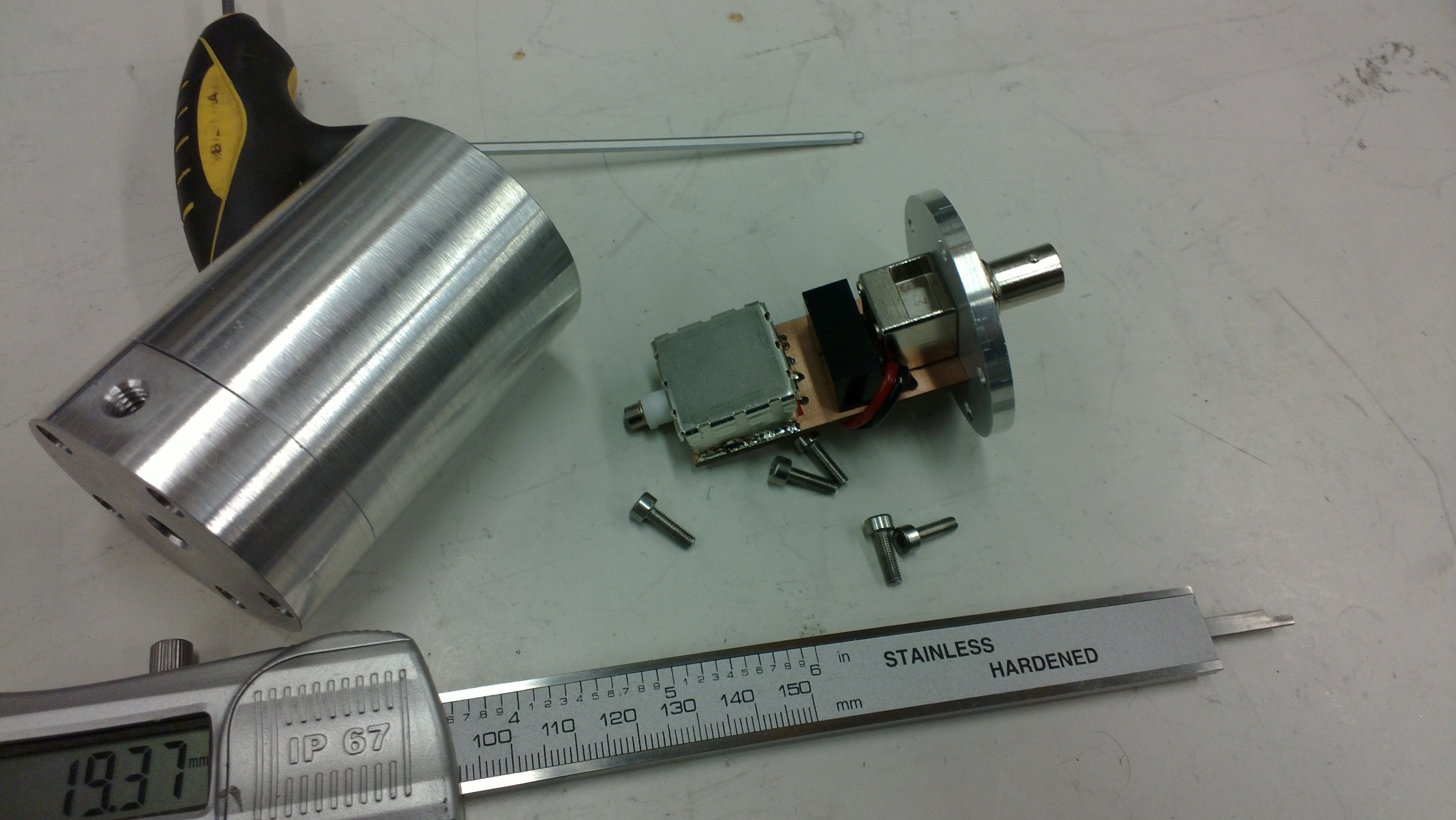
Here two holes have been drilled in to the back-plate for the BNC-commector (ca 12.2 mm diameter) and a DC-input jack (5.5mm diameter with a 2.5mm pin). The PCB is attached to the back-plate and slides into the body, while the photodiode looks out through the hole of the face-plate.
The only setback was a disagreement between the 1-2-3 pin-sequence in the datasheet vs. my PCB-software for the SOT-89 packaged 7905 negative voltage regulator. If you look closely you can see it is soldered up-side-down on this board because the PCB footprint is wrong.
What you want to solder larger things with a smaller iron is a hot air bath. Used correctly it will also reduce thermal shock on the smaller parts and give you higher long term reliability.
On the BNC it would not help but on the shielding can it will.
It makes a world of difference.